In one case of flexible microstrip, changing the fabrication process produced a clearly lower insertion loss, yet the report attributed the improvement solely to "a smoother copper surface." That conclusion may be premature: if the conductor cross-section, adhesive layers, and surface condition all changed together, you cannot credit the entire improvement to a single factor. Reading a loss report means more than finding the lower curve—you must determine which variables the comparison actually isolated. The study by Woo et al. (2022) on flexible microstrip, which provides both cross-section scans and physical test data, is a useful example for practicing this kind of judgment.
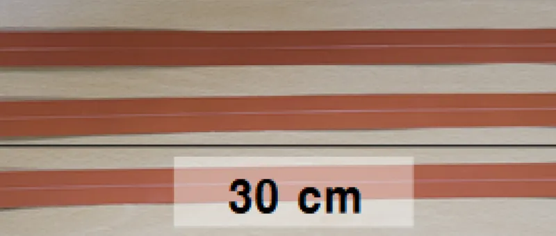
Figure 1 | Detail of a conventional-process flexible microstrip sample used for insertion-loss comparison.
First look at cross-sections: the photos already expose variables
Figure 2 is not simply a "rough copper vs. smooth copper" comparison. The left sample shows pronounced undulation at the conductor bottom, while the right sample is not only smoother but also has an arched cross-section profile. If you only highlight the rough surface and ignore the profile change, you have already discarded another potential contributor to loss at the first step of interpreting the images.
High-frequency conductor loss depends on how current is distributed. Surface condition affects current flow near the conductor surface; corner sharpness and arching change local current concentration. Both effects can contribute to the result, but "may contribute" is not the same as "have been separately quantified." The magnitude of each effect also depends on the actual copper foil, frequency, and stackup.
When annotating the report, first record the facts that are clearly visible in the photos: the surfaces differ, and the profiles differ. Then list items that cannot be confirmed from the images alone for follow-up, such as the measured roughness metrics, sampling locations, and statistical coverage. Do not draw quantitative conclusions about an entire reel of foil from a single local SEM image.

Figure 2 | Copper conductor cross-sections for the two processes: left shows a rougher bottom surface; right exhibits both a smoother surface and an arched profile.
Treat the shape scan as an independent measure
The authors use α to denote the ratio of bottom trace width to top trace width. When α equals 1 the profile is close to rectangular; as α decreases the arch becomes more pronounced. This parameter is important because it converts a qualitative "looks rounder" observation into a geometric input that can be scanned, allowing the same simulation framework to show how shape alone affects results.
In Table 2 of the original paper, at 10 GHz α changes from 1 to 0.26 and the loss per unit length changes from 0.266 to 0.235 dB/cm, a difference of 0.031 dB/cm. That set of numbers answers the question of how cross-section change affects loss within that model. It is not a universal benefit for all materials, nor should it be applied directly to promise a specific channel loss reduction on any high-speed board.
Figure 4 shows the corresponding simulated current-density distributions: the rectangular cross-section has more pronounced local concentration, while the arched section redistributes the current. Here one should say "the model supports that shape affects current distribution," not "the instrument has measured current flowing exactly along these colors." Heat maps and measured curves are different types of evidence and should be labeled separately in the report.
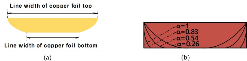
Figure 3 | Cross-section parameter α equals bottom width divided by top width; decreasing α changes the cross-section shape.
Measured improvement is larger — don't rush to assign credit
In physical tests, two types of 30 cm samples show insertion loss per unit length around 0.66 and 0.37 dB/cm at 10 GHz. This change is much larger than the cross-section scan difference above, but you cannot infer from that that "the remaining portion must all come from roughness." The model and the samples are not separated by only a single unknown variable.
The original paper's Table 3 also lists structural differences: the adhesive/laminate configurations of the two process samples are not identical. The dielectric environment participates in the field distribution and therefore affects loss. Thus the measurements demonstrate that the specific samples with their complete structures differ under the test conditions, not that the study has allocated quantified contributions to roughness, cross-section, and dielectric individually.
The authors also note that the loss tangent used in the model was measured at 2 GHz but applied at higher frequencies, which may contribute to the discrepancy between simulation and measurement. Readers need not reject the entire study for that reason; the correct approach is to retain the useful comparisons while narrowing the scope of conclusions. A model that explains trends does not imply that absolute values at every frequency point are closed.
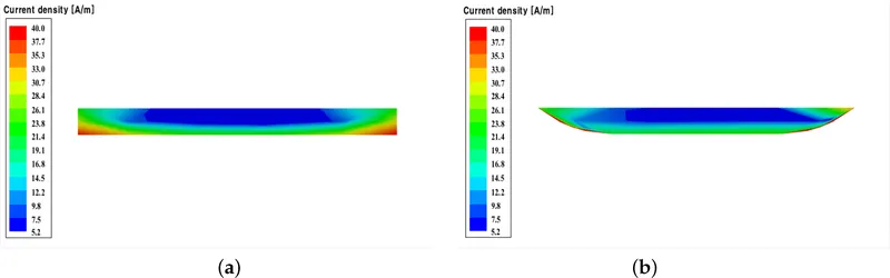
Figure 4 | Simulated current density at 10 GHz: local concentration differs between rectangular and arched cross-sections.
Review with a two-column comparison table
Next time you receive insertion-loss reports for process A and B, create a side-by-side list of trace length, trace width, copper thickness, cross-section profile, roughness metrics, dielectric and adhesive stackup, test frequency range, calibration, and adapter/connectivity structures. Check identical items and separately circle differing items. If you circle three or four items at once, write the conclusion as an "overall process comparison" rather than claiming "a single material parameter determines the result."
Also align the vertical-axis definition: is the plot showing the total dB for the whole channel, or normalized dB/cm? Have connector and adapter losses been removed? You cannot simply divide the total loss of a short line that includes adapters by its length and assume the result is directly comparable to the loss of a long trace without adapters. If conditions are not aligned, even a correctly labeled unit can be misleading.
If the goal is only to select a usable process, an overall comparison can be valuable; if the goal is to optimize a specific parameter, you need additional single-variable samples or a validated model. Be explicit about whether you are aiming to choose between processes or attribute cause, so you know whether the existing reports are sufficient.
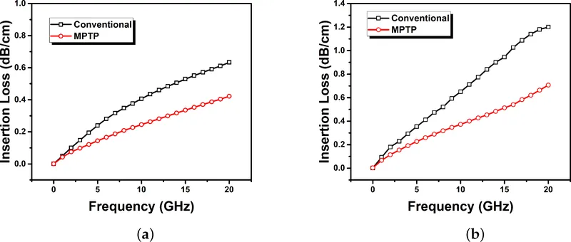
Figure 5 | Insertion-loss comparison per unit length for the two processes: left is simulation, right is measurement; the two types of curves are different forms of evidence and should not be conflated.
The ability to read loss reports lies in knowing what each curve can and cannot demonstrate. For the next review, prepare a two-column conditions table, then separate conclusions into "model single-variable results" and "physical overall results." Don't be quick to give full credit to a single factor — the two curves you are comparing may have changed only the copper surface, or they may have changed cross-section and stackup as well.