Hazards of PCB Warpage
On automated surface-mount assembly lines, an uneven PCB causes pick-and-place misalignment and can prevent components from being accurately placed into through-holes or onto surface-mount pads; in severe cases it may damage automated insertion equipment. After components are soldered, a warped board makes component leads difficult to trim uniformly and may prevent the board from being installed into chassis or mating connectors. For assembly shops, warped boards are a major headache.
Modern SMT processes increasingly demand higher placement accuracy, speed, and automation, which places stricter flatness requirements on PCBs.
IPC standards specifically indicate that PCBs with surface-mount devices are allowed a warpage of 0.75%, while PCBs without surface-mount devices may be allowed up to 1.5% warpage. In practice, to meet high-precision and high-speed assembly requirements, some assemblers require stricter limits such as 0.5% or even 0.3% in certain cases.
PCBs are composite structures of copper foil, resin, and glass fiber; these materials have different physical and chemical properties. When laminated together, residual thermal stresses are inevitably introduced and can lead to warpage. In addition, high-temperature processing, mechanical cutting, and wet processes during PCB fabrication also significantly affect board deformation. The causes of PCB warpage are therefore complex; reducing or eliminating warpage caused by material differences or processing remains a major challenge for PCB manufacturers.
Analysis of Causes of PCB Warpage
PCB warpage should be analyzed from material, structure, pattern distribution, and process perspectives. The following sections summarize common causes of warpage and corresponding mitigation ideas.
Uneven copper pour areas worsen bending and warpage
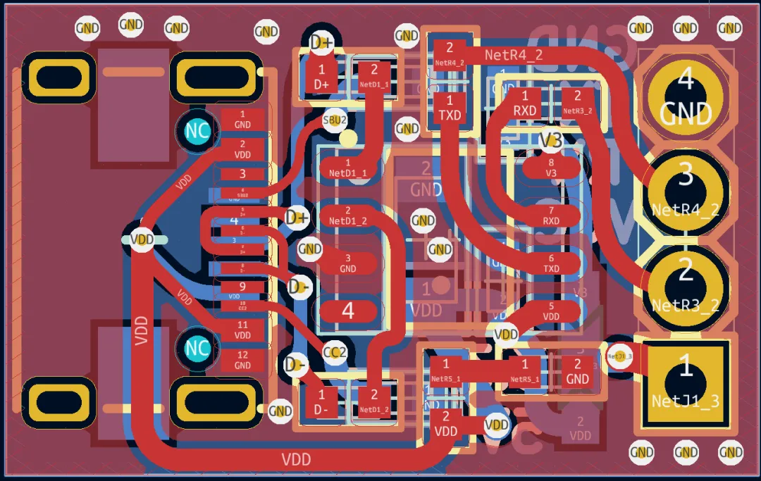
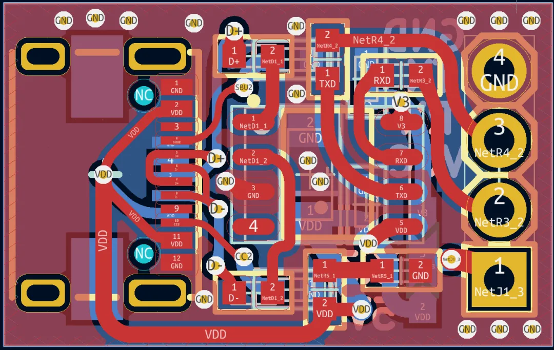
Large copper planes are commonly used for ground and sometimes Vcc. When large copper areas are not symmetrically distributed across the board, non-uniform heat absorption and dissipation occur. The board expands and contracts with temperature; if different regions expand or contract at different rates, they generate differential stress and deformation. If the board temperature reaches the upper limit of Tg, the laminate will begin to soften and warp.
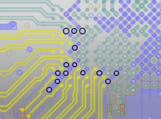
Inter-layer connections (vias) constrain board expansion and contraction. Modern PCBs are mostly multilayer and contain through, blind, and buried vias that act like rivets. These connections locally restrict thermal expansion and can indirectly contribute to bending and warpage.
Common causes of warpage
- Board self-weight causing sag
PCBs conveyed through reflow ovens are typically supported at the board edges by the conveyor. If heavy components are mounted on the board or the board is very large, the board can sag in the center under its own weight, causing bending.
- V-cut depth and breakaway tabs on panelized boards
V-cuts (score lines) inherently weaken the panel structure because they cut grooves into a larger sheet. Areas near V-cuts are prone to deformation, and the depth and remaining tab width affect panel warpage after singulation.
Effects of lamination materials, structure, and copper patterns
PCBs are formed by laminating cores, prepregs, and outer copper foil. During lamination these materials experience heat and may deform. The amount of deformation depends on the coefficient of thermal expansion (CTE) mismatch between materials.
Typical CTE values: copper foil CTE ≈ 17 × 10-6 /°C. For common FR-4, Z-direction CTE below Tg is about (50–70) × 10-6 /°C and above Tg about (250–350) × 10-6 /°C. X-direction CTE is similar to copper due to the presence of glass fiber.
Manufacturing-Induced PCB Deformation
Deformation arising during PCB fabrication is driven by both thermal and mechanical stresses. Thermal stress primarily occurs during lamination; mechanical stress results from stacking, handling, and baking. The following process steps are commonly associated with warpage generation.
1. Incoming copper-clad laminate (CCL)
Standard CCL is usually symmetric double-sided laminate with no copper pattern. Copper foil and glass-fiber-based CTEs are similar, so lamination itself rarely causes CTE-related deformation. However, large laminating presses can have temperature gradients across the hot plates. Different regions may cure the resin at slightly different rates and exhibit different dynamic viscosities during heating, producing local stresses. These residual stresses may initially be balanced but can gradually release during later processing and cause warpage.
2. Lamination
Lamination is the primary source of thermal stress. Compared to single-sided copper-clad laminates, completed multilayer PCBs are thicker, have more varied copper patterns, and use multiple prepregs, so they develop more complex thermal stresses that are harder to eliminate. Stresses trapped in the board can be released later during drilling, routing, or baking, producing deformation.
3. Solder mask and legend curing
Solder mask inks cannot be stacked during curing, so panels are often placed vertically in racks for oven curing. Solder mask cure temperatures are around 150 °C, which may exceed the Tg of medium- and low-Tg materials. Above Tg the resin is in a high-elasticity state and is more prone to deformation under self-weight or oven airflow, causing warpage.
4. Hot-air solder leveling (HASL) / wave soldering impacts
Typical HASL process parameters for standard boards: pot temperatures around 225–265 °C, immersion time 3–6 s; hot-air knife temperatures around 280–300 °C. Boards go from room temperature into a high-temperature solder bath and are often rinsed within two minutes after exiting. This is a severe rapid-heating and rapid-cooling cycle. Because PCB materials and structures are non-uniform, thermal stress develops during these cycles, causing microscopic strains and macroscopic warpage.
5. Storage
Work-in-progress PCBs are typically stored vertically in racks. Improper rack spacing or stacking during storage can introduce mechanical deformation, especially for boards thinner than 2.0 mm.
Preventing PCB Warpage
Board warpage significantly affects PCB manufacturability and downstream assembly. A warped board may make soldering unreliable, impede connector mating, and disrupt subsequent processes. As assembly technologies continue to require higher flatness, identifying and controlling the causes of warpage is critical.
Design and material considerations
- Symmetric prepreg/core stack-up
Arrange prepreg and core layers symmetrically. For example, on a six-layer board the thickness and number of prepreg sheets between layers 1–2 and 5–6 should match; otherwise post-lamination warpage is likely.
- Use the same supplier for core and prepreg
Where possible, source multilayer cores and prepregs from the same supplier to improve material consistency.
- Balance outer-layer copper
A-side and B-side copper pattern areas should be as close as possible. If one outer layer has a large copper pour and the other only a few traces, the board is prone to warp after etching. If copper area is imbalanced, add isolated copper grid patterns on the sparse side to balance the thermal/mechanical effects.
Process and handling recommendations
- Prebake before cutting (depaneling)
Prebake CCL prior to cutting at ~150 °C for about 8 ± 2 hours to remove moisture and to further cure resin, reducing residual board stress. Many manufacturers use prebake times ranging from 4–10 hours depending on the board class and warpage tolerance; decide prebake duration based on product requirements.
- Prefer baking after panel singulation
Both approaches (bake before or after depaneling) can work, but baking after cutting is generally recommended. Inner-layer cores should also be baked when appropriate.
- Respect prepreg machine-direction (MD) and transverse-direction (TD)
Prepreg shrinkage differs between MD and TD. During cutting and stacking, distinguish MD from TD; incorrect orientation or random stacking of prepreg layers is a common cause of multilayer warpage. Typically, the roll direction of prepreg is the machine direction (MD) and the width direction is the transverse direction (TD). For copper-clad laminates, the long side is usually the TD and the short side the MD, but confirm with your supplier if uncertain.
- Post-lamination stress relief
After hot and cold pressing, trim flash and place boards flat in an oven at 150 °C for about 4 hours to allow trapped stress to release and the resin to fully cure. This step should not be omitted.
- Straightening during plating for thin boards
For ultra-thin multilayer boards (0.4–0.6 mm), use specialized clamps and straightening fixtures during panel electroplating. On automatic plating lines, mount thin panels in fixtures that are clamped together on a rod so the entire run is straightened; this prevents deformation after adding 20–30 μm of plated copper. Without straightening, thin boards will bend after plating and are difficult to remedy.
- Controlled cooling after HASL
After passing through the solder pot (~250 °C), place boards on a flat, rigid surface such as a marble or steel plate for natural cooling before cleaning, or use an air-float cooling bed. Some factories quench boards in cold water to enhance solder brightness; this rapid hot-to-cold shock can induce warpage, delamination, or blistering in certain board types and is not recommended.
- Storage and handling
Adjust rack spacing appropriately, avoid improper stacking, and handle thin boards with extra care to prevent mechanical deformation caused by storage or transport.
Treatment of warped boards
In well-managed factories, boards undergo 100% flatness inspection at final inspection. Nonconforming boards are segregated and often placed under heavy, flat plates in an oven at 150 °C for 3–6 hours, cooled under pressure, then rechecked. Some boards require two or three bake-and-press cycles to recover; if preventive process controls are not implemented, baking alone may not save the board and scrapping may be necessary.
PCB Warpage Standards and Measurement
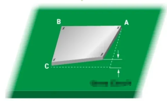
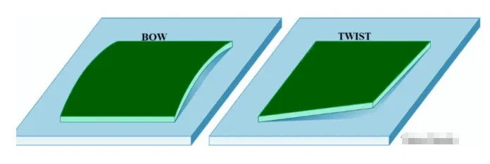
PCB warpage refers to the deviation of a board from flatness — for example, when a board placed on a flat table has its corners touching but the center arches upward. Industry measurement method: lay the board flat with all four corners touching the table, measure the height of the center arch. Warpage percentage is calculated as:
Warpage (%) = (arch height / PCB long-edge length) × 100%
According to IPC-6012 (1996 edition) for rigid PCBs, the allowable maximum warpage and twist is between 0.75% and 1.5%, depending on product class and process capability. Most manufacturers control warpage for standard 1.6 mm double- or multilayer boards to roughly 0.70–0.75%. Many SMT and BGA boards require warpage within 0.5%, and some manufacturers with stronger process control can achieve 0.3%.
Summary: Key Actions to Avoid PCB Warpage in Manufacturing
- Design: arrange prepreg and core layers symmetrically; use cores and prepregs from the same supplier when possible; balance outer-layer copper patterns or add isolated copper grids to even copper area.
- Prebake: bake panels before cutting at ~150 °C for typically 6–10 hours to remove moisture and reduce internal stress; apply to inner layers and double-sided boards as needed.
- Prepreg orientation: confirm and align MD/TD correctly before stacking and lamination.
- Post-lamination stress relief: perform flat oven baking (e.g., 150 °C for ~4 hours) after trimming/milling flash.
- Drilling prebake: prebake before drilling (e.g., 150 °C for ~4 hours) when appropriate.
- Thin-board plating: avoid mechanical brushing when possible; use chemical cleaning and dedicated fixtures to prevent bending during plating.
- HASL cooling: allow boards to cool on a flat, rigid surface or use air-float cooling, and avoid immediate cold-water quench after HASL.
Implementing these material selection, design, process-control, and handling measures helps minimize residual stress, avoid thermal-mechanical shocks, and reduce PCB warpage, improving assembly yield and product reliability.