










Impedance targets that look correct in the design tool frequently miss on the finished flexible circuit. The gap between simulated and measured values is one of the more persistent FPC impedance control issues.
Flexible PCB 100 ohm impedance is especially sensitive. Small changes in dielectric thickness, copper geometry, or material properties push the result outside the usual ±10 % window. Most failures originate in the inputs given to the stack-up rather than in the etching process itself.
What the Design Must Provide for Impedance Control
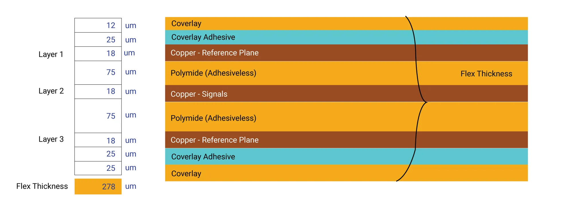
Accurate impedance starts with complete and realistic design inputs. The fabricator needs the exact dielectric materials, their thicknesses, the copper weight, the target impedance (single-ended or differential), the reference plane configuration, and whether coverlay or adhesive is present over the traces.
Missing or idealized data is the most common starting point for failure. Using a generic polyimide Dk instead of the specific grade, ignoring the adhesive layers, or assuming the coverlay has no effect on microstrip structures all produce optimistic simulations that the production process cannot match.
The design must also state the tolerance. A ±10 % window is typical; tighter requirements demand tighter process control and usually higher cost. Without a clear tolerance the fabricator cannot know whether a measured 92 Ω result on a 100 Ω target is acceptable.
How Material, Copper Thickness, and Line Width Drive Impedance
Three physical variables dominate FPC impedance.
Dielectric thickness and Dk. Polyimide and adhesive layers are thinner and more variable than FR4 prepreg. A 10 µm change in adhesive thickness produces a measurable shift in impedance. Material lots also vary in Dk; using a datasheet typical value instead of the actual production lot data introduces error.
Copper thickness. Finished copper weight after plating or etching is not identical to the nominal starting foil. On thin flex the percentage variation is larger. Thicker copper lowers impedance for a given line width; thinner copper raises it.
Line width and spacing. Etching tolerance on flexible material is often ±10–20 % of the nominal width for fine lines. Differential pairs are particularly sensitive to both width and the gap between the two conductors. A few microns of under- or over-etch moves a 100 Ω pair outside specification.
These three factors interact. A simulation that assumes perfect geometry and nominal material values will not survive the real process window.
Why 100 Ω Differential Impedance Is Difficult to Hold
100 Ω differential is a common target for high-speed interfaces. On FPC it is harder to control than the same target on rigid FR4 for several reasons.
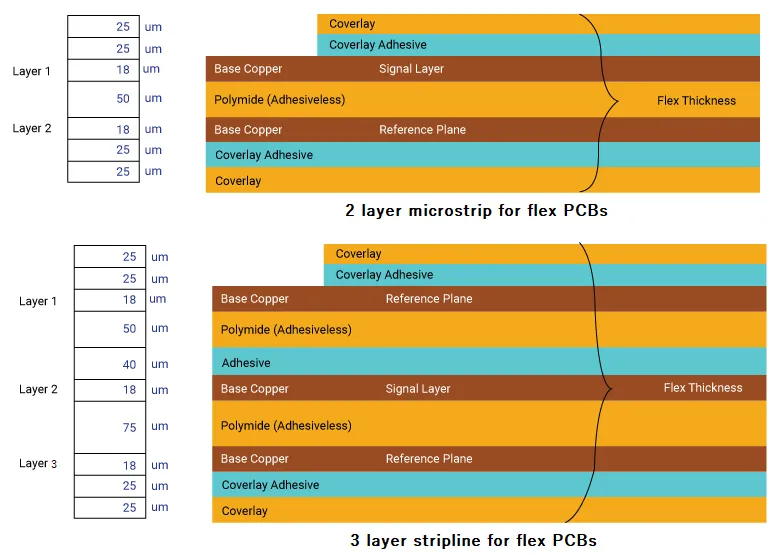
The dielectric is thinner, so the same absolute thickness variation produces a larger percentage change. Coverlay or additional adhesive layers over microstrip pairs alter the effective dielectric and are often omitted from early simulations. The flexible material also stretches and moves slightly during processing, changing the final geometry relative to the artwork.
Etching compensation that works for rigid boards is frequently insufficient for flex. The etch factor is different, and the thin copper foil responds more quickly to process changes. As a result, a line width that calculates to 100 Ω in the tool may measure 90 Ω or 110 Ω on the finished panel.
When the design also includes transitions from flexible to rigid sections, or changes in reference planes, the impedance discontinuity adds further measurement variation on test coupons.
Simulation Accuracy and Production Adjustment Process
Good simulation requires the actual stack-up that will be built, not a simplified version. That means correct polyimide thickness, adhesive thickness and type, coverlay presence, copper weight after processing, and realistic etch factors.
Even with accurate inputs the first articles often need adjustment. Fabricators run impedance coupons, measure the result, and then modify the artwork line width or the process parameters for subsequent panels. This compensation loop is normal for FPC. Designs that leave no margin for adjustment, or that treat the first simulation as final, frequently fail to meet the target in volume.
The adjustment process works only when the coupon design represents the actual routing environment. Coupons placed in unrealistic stack-up regions or with different coverlay conditions produce misleading data. The production adjustment then corrects the wrong variable.
Common Sources of Impedance Failure in Manufacturing
Several recurring mistakes explain most out-of-spec results.
Using rigid-board dielectric values or stack-up assumptions for a flexible construction. Ignoring the coverlay or bonding adhesive over the traces. Specifying line widths without process-compensated etch factors. Providing incomplete material callouts so the fabricator substitutes a similar but not identical dielectric. Placing impedance-controlled traces in regions where the reference plane is discontinuous or the dielectric thickness changes.
Any one of these inputs can shift a 100 Ω target by more than the allowed tolerance. Combined, they make the measured result unrecognizable relative to the original simulation.
Late changes to the stack-up after the impedance calculation is frozen are another frequent cause. Adding or removing coverlay, changing adhesive thickness, or altering copper weight after the line widths have been set guarantees a mismatch.
Practical Steps That Improve First-Pass Success
Lock the complete stack-up, including coverlay and adhesives, before running final impedance calculations. Use material data from the actual supplier and grade that will be purchased. Apply realistic etch compensation based on the fabricator’s process capability for flexible material, not generic rigid-board factors.
Design test coupons that match the production stack-up and routing style. Allow the fabricator a compensation loop on the first panels. Specify a workable tolerance; ±10 % is achievable on most FPC constructions, while ±5 % requires tighter process control and higher cost.
When the design contains both flexible and rigid-flex regions, calculate and control impedance separately for each environment. Transitions should be managed so they do not dominate the coupon measurements.
Engineering Takeaway
FPC impedance control fails most often because the design inputs do not match the physical stack-up and process variation that actually occur in manufacturing. Material thickness, copper geometry, and dielectric properties all move more on flexible circuits than on rigid boards.
Flexible PCB 100 ohm impedance is particularly exposed to these variations. Accurate stack-up data, realistic etch factors, proper coupon design, and a planned compensation step are required to keep the measured result inside specification. Treating impedance as a pure calculation rather than a process-controlled outcome is the root of most FPC impedance control issues.






