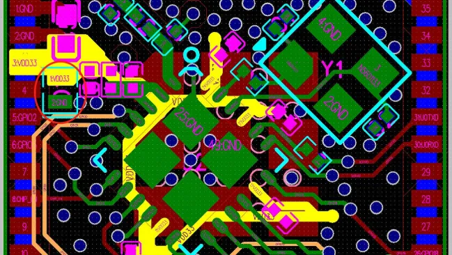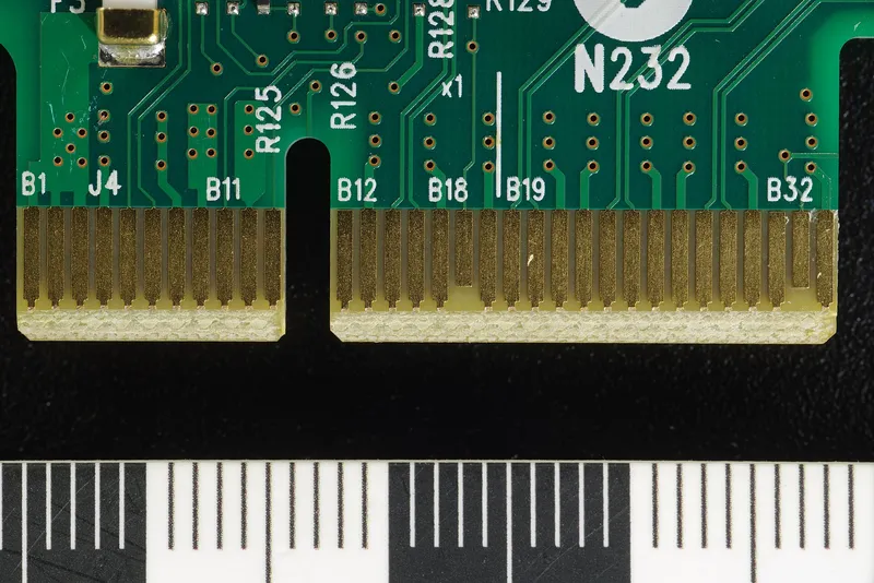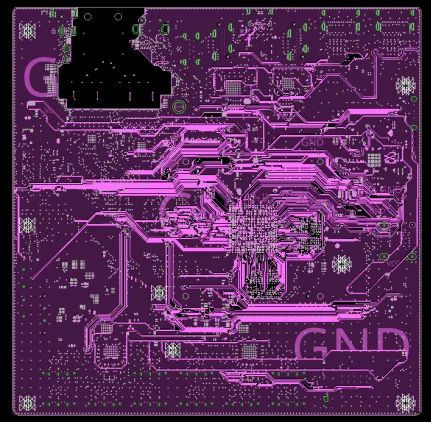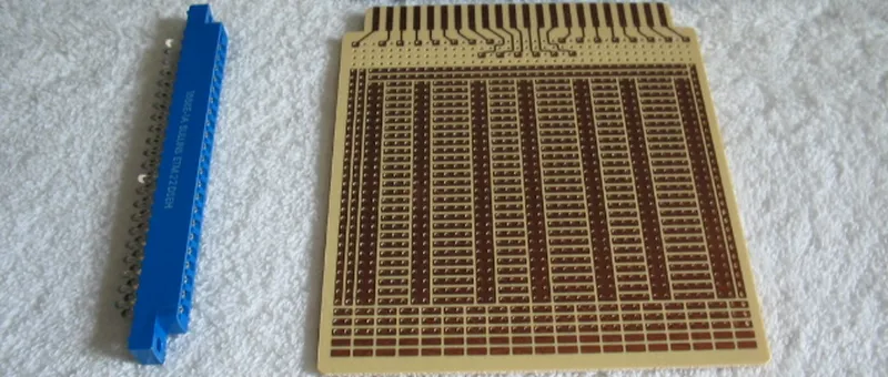
The connector outline, gold-finger pitch, and surface finish can all be drawn correctly, and a 3D check can show a clean insertion, yet review still requires the inner-layer copper under the fingers to be pulled back as a block. That step is not for a cleaner-looking board edge. It serves bevel machining, edge tolerance, metal-debris risk, and high-frequency structural consistency at the same time. Treat the gold-finger region as a special electromechanical interface. Do not review only the top-layer contact pads. The copper that cannot be seen on the top layer is what most often creates risk at both the machined edge and the insertion area.
Treat Gold Fingers as an Interface That Will Be Machined
An ordinary pad is rarely cut again after fabrication. Gold fingers still see outline routing, a bevel or chamfer, insertion, and long-term wear. When the bevel tool enters from the board edge, board-thickness tolerance, layer-to-layer misregistration, and cut depth all change how close the tool comes to inner-layer copper. If an inner plane runs all the way to the edge, the mildest result is exposed copper on the edge. Worse, copper chips, burrs, or interlayer residue from cutting can sit next to adjacent contacts. Review must overlay the outline, bevel zone, gold-finger mask opening, inner-layer pullback, and connector housing at once, not layer by layer in isolation.
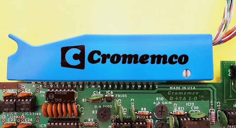
Inner-Layer Pullback Is Not Only a Short-Circuit Fix
Even if the bevel never cuts copper, a large inner plane near the edge still changes the electric field and impedance in the gold-finger region. If high-speed differential contacts suddenly meet a different reference structure in the insertion zone, the reflection can exceed the effect of a small trace-width error. A large copper area beside a power contact also changes coupling to nearby signals. Pullback distance cannot be copied as a fixed number without the interface data rate and the connector definition. Low-speed control interfaces care more about machining and insulation. High-speed interfaces also need the keep-out, reference-layer, and return-path rules from the connector manufacturer.
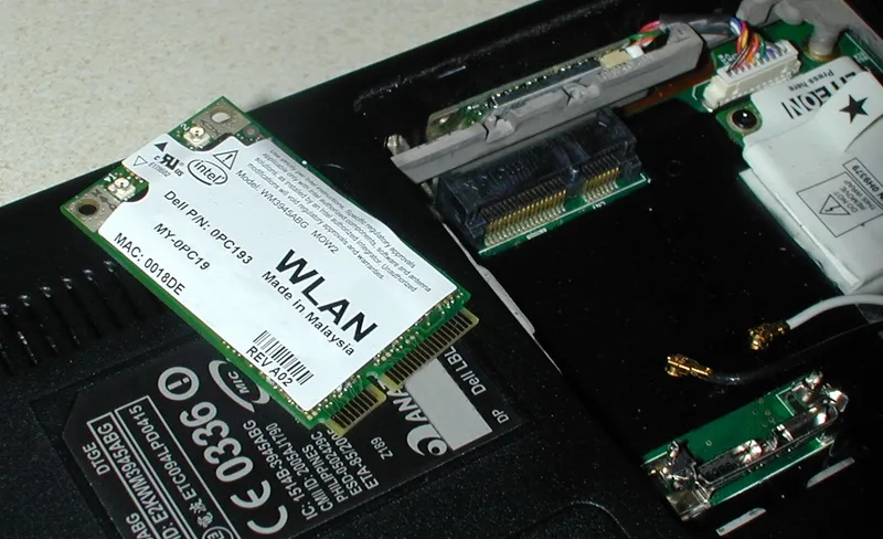
Full Mask Openings and Copper Pullback Must Be Checked by Layer
A full solder-mask opening on the top layer keeps mask bridges from peeling under repeated insertion and keeps coating off the contact surface. Inner-layer pullback is a stackup constraint for machining and electrical behavior. One does not replace the other. State clearly in the fabrication notes whether the bottom side also has gold fingers, whether both sides need a bevel, and whether the plated area includes plating tails. Near the outline, also check test points, vias, chassis-ground screws, and shield pads for intrusion into the real bevel and connector envelope. A clean top-layer opening does not prove a multilayer board is safe.
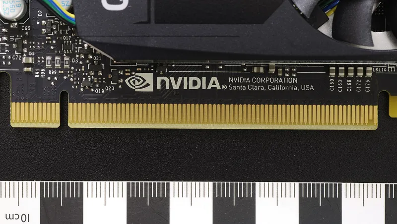
Run a Reverse Check Before Release
Hide top-layer copper and display every inner layer with the outline. Look for any plane, teardrop, or pour that still crosses the pullback boundary. Then hide the inner layers and inspect only solder mask, surface finish, and bevel callouts. Put the connector 3D envelope and board-thickness tolerance into the assembly check and confirm insertion depth and contact location. Gerber review should also watch negative planes, dynamic copper, and refill after a re-pour, so an outline change does not silently void an old keep-out. If manufacturing data was converted across EDA versions, measure board-edge-to-copper distance again on the final plot data.
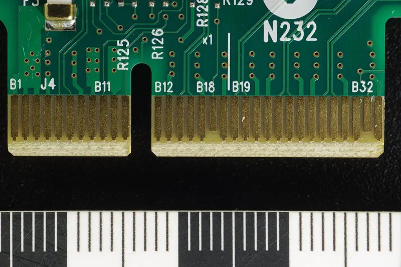
Give Fabrication Notes That Can Be Executed
Do not write only "process gold fingers as usual." State board thickness, surface finish, bevel angle or depth, whether both sides are beveled, allowed edge burr, and which mechanical datum defines the inner-layer copper keep-out. If the connector specification gives recommended edge geometry, bind that revision number to the review record. On first articles, measure pitch and plating, then inspect the edge for exposed copper, delamination, or burrs, and check insertion and contact location with the actual connector. Any production change that touches the outline, stackup, or copper-pour strategy should reopen this review. Do not reuse an old conclusion that "gold fingers were already checked."
Keep the fabricator's replies on bevel capability and inner-layer registration tolerance in the review record. If the same interface moves to a different thickness, layer count, or connector, the old pullback distance is only a starting point. It should not be copied directly. In the EDA tool, a dedicated gold-finger rule region can place every signal layer, plane layer, and dynamic pour under the same keep-out, then measure outline-to-nearest-copper after plotting. Later re-pours or outline edits then raise an error instead of waiting for a CAM engineer to notice by habit.
Gold-finger review can be fixed as three plots: outline and bevel, inner-layer pullback on every layer, and solder mask plus surface finish. Use the same coordinate datum on all three. Problems show up faster than hunting layer by layer in the full board. If a fabricator query only asks whether exposed copper is allowed, do not answer yes or no in isolation. Return to the connector structure and the product's insulation requirement. Process capability, design intent, and acceptance criteria belong in one statement, or production will interpret them separately.
Correct gold-finger dimensions are only the start. Stable insertion depends on the interface formed by edge machining and every copper layer together.