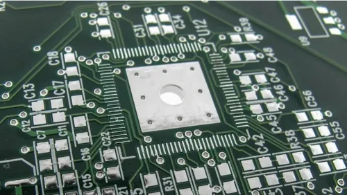
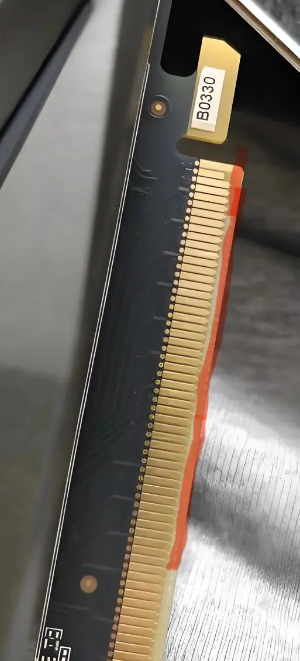
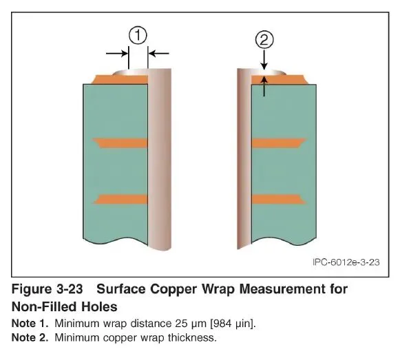
Using solder mask to create PCB characters through exposure and development, instead of using conventional screen printing, is a viable high-precision solution for fine lettering. The resulting characters are formed from cured photosensitive solder mask itself rather than from a separate silkscreen ink layer.
This process can solve the resolution limitations of conventional screen printing, but it also introduces stricter design and manufacturing constraints. The most important trade-off is that solder-mask characters usually have lower visual contrast than conventional silkscreen. When dedicated character-jetting equipment is unavailable, however, exposure-developed solder mask can be considered for applications that require very small lettering.
Advantages of Using Solder Mask for PCB Characters
1. High Line Resolution for Fine Characters
Conventional screen printing typically reaches a minimum line width of approximately 0.15 mm. When the line becomes narrower, the ink may break, smear, or fail to transfer uniformly through the screen. The achievable resolution is affected by screen mesh, ink rheology, printing pressure, and process alignment.
With solder-mask exposure and development, the resolution is primarily determined by the phototool, exposure capability, solder-mask imaging performance, and development control. The process can generally produce lines as narrow as 0.1 mm, and potentially finer lines under suitable conditions. This makes it more appropriate for densely populated PCBs where reference designators, polarity marks, or other identification characters must fit into a limited area.
Fine-line capability does not mean that every font or character shape will be manufacturable. Very narrow strokes, small enclosed areas, and sharp corners remain sensitive to exposure and development conditions. Character geometry should therefore be reviewed against the actual manufacturing capability rather than evaluated only from the CAD artwork.
2. A Flatter Surface
Because the character is made from solder mask, its thickness is closely related to the surrounding solder-mask layer. It does not create the additional raised profile associated with a separate screen-printed ink layer.
This lower profile can reduce the risk of a local "standoff" effect beneath fine-pitch components. A thick silkscreen feature located under or near a component may affect placement flatness or interfere with the formation of small solder joints. A solder-mask character is less likely to create this type of local height difference, provided that its location and opening structure are properly designed.
3. Accurate Positioning and Strong Adhesion
Solder-mask characters are formed using imaging and registration rather than by positioning a separate screen-printing operation. Their positional accuracy can therefore be significantly better than that of conventional silkscreen characters.
After UV curing and thermal processing, the solder mask has good adhesion and resistance to heat and chemicals. It is generally better able to withstand flux, cleaning agents, and lead-free reflow processing without discoloration, blistering, or peeling. The actual result still depends on solder-mask chemistry, surface preparation, curing conditions, and process control.
4. Fewer Separate Manufacturing Operations
When the character pattern is incorporated into the solder-mask imaging process, a separate character screen-printing and baking operation can be eliminated. This reduces the number of handling steps and lowers the risk of contamination or board damage caused by additional movement between processes.
The reduction in process steps can also improve production consistency because the character layer no longer depends on a separate screen, ink deposition condition, or printing alignment operation.
5. Consistent Character Quality
This method avoids several common screen-printing defects, including blocked mesh openings, uneven ink transfer, screen marks, and local variations in deposited ink thickness. Line consistency from panel to panel can therefore be better than with conventional screen printing.
It can also reduce the risk of silkscreen ink extending onto the edge of a pad. Nevertheless, the character artwork must still maintain adequate clearance from pads and other surface-finished areas. Better imaging accuracy does not eliminate the need for appropriate design rules.
Disadvantages and Design Constraints
1. Less Layout Freedom
A solder-mask character must be incorporated into the solder-mask artwork rather than placed on an independent silkscreen layer. This creates more constraints on character placement.
If a conductor is located beneath a character region, that conductor may be covered by the character solder mask. In areas where the background is intended to be a solder-mask opening, the exposed region may instead reveal the substrate or copper surface. Unintended exposed copper must be avoided because it can increase the risk of short circuits, oxidation, or other reliability problems.
As a result, text cannot always be positioned as freely as conventional silkscreen. Designers must evaluate the character, solder-mask openings, copper features, and adjacent pads as one combined pattern.
2. The Character Must Not Cover a Pad
Silkscreen overlapping a pad may create an appearance or solderability concern, but some manufacturing situations can tolerate a limited amount of silkscreen-to-pad overlap. A solder-mask character is different. If it covers a solderable pad, that portion of the pad becomes unavailable for soldering and forms a functional dead area.
For this reason, solder-mask characters must be kept completely clear of pads and other surface-finished regions. This requirement is more restrictive than the clearance normally applied to silkscreen. The rule is particularly important for small pads, fine-pitch packages, test points, and exposed contacts.
3. Local Rework Is Extremely Difficult
If a screen-printed character is incorrect, it can often be removed with a suitable solvent and printed again with limited impact on the board. A solder-mask character becomes permanently integrated after exposure, development, and curing. It cannot normally be removed locally without damaging the surrounding solder mask or the copper beneath it.
Attempting to scrape away an incorrect character may expose or damage the copper surface and can compromise the insulation function of the solder mask. In practice, a serious artwork error may make the entire board difficult or impossible to recover. Character data should therefore receive the same type of pre-production review as other solder-mask artwork.
4. Photolithography Risks with Fine Features
Very fine character lines are sensitive to the imaging profile. Where the underlying copper is relatively thick, the sidewall geometry can reduce the effective exposure or development margin. The resulting line may become narrower than intended, or a very fine feature may break completely.
This behavior is related to the interaction between copper topography, solder-mask thickness, exposure energy, phototool resolution, and development compensation. Production may need tighter control of exposure and development parameters than would be required for ordinary solder-mask openings. The design should therefore be verified against actual process capability, especially when character strokes are close to the lower limit of the process.
5. Dependence on the Copper Structure Beneath the Character
To improve character visibility, a solid copper area is sometimes placed beneath the character as a background. This can make the character easier to distinguish, but it also increases the copper area in a region that may not require it electrically.
On high-frequency or impedance-controlled boards, additional copper can affect the local electromagnetic environment. Depending on the geometry, it may slightly influence signal behavior, impedance, or antenna-like coupling. These effects may be small, but they should be reviewed for precision RF designs and other circuits with demanding signal-integrity requirements.
A solid copper background should therefore not be added automatically. Its effect on adjacent traces, reference-plane continuity, clearance, and local thermal behavior should be considered during layout.
Cross-Hatch Adhesion Performance
1. Integrated Solder-Mask Structure
Conventional silkscreen ink is deposited on top of the solder mask or substrate as a separate material. A character formed by solder-mask exposure and development is part of the solder-mask structure itself. After curing, it forms an integrated crosslinked film with the surrounding solder mask or, where the character is formed over an opening, with the prepared copper or substrate surface.
During a cross-hatch adhesion test, the surface is cut into a grid and pulled with adhesive tape. Because the character is not simply a separate printed layer, the cut edges generally show little tendency to peel when the solder-mask process and surface preparation are properly controlled. The result can reach the highest 5B classification, indicating no visible coating removal, although the actual rating remains dependent on the material and manufacturing process.
2. Resistance to Thermal and Chemical Exposure
After lead-free reflow and flux cleaning, a properly cured solder-mask character generally retains its adhesion well. By comparison, some low-quality white silkscreen inks may become brittle after thermal exposure and show more peeling during a subsequent cross-hatch test.
Good adhesion depends on more than the character-generation method. Copper cleanliness, surface roughening, solder-mask curing, exposure, development, and final thermal treatment all affect the result. A process review should therefore evaluate the complete material and manufacturing stack rather than treating the imaging method as the only determining factor.
Special Considerations for Cross-Hatch Testing
Characters located directly on exposed copper require particular attention. For example, a character may be formed over copper that has already received a surface finish. In this case, adhesion depends on the solder mask's ability to bond to that finished copper surface.
PCB fabrication processes commonly include copper pretreatment or roughening before solder-mask application. When this preparation is properly controlled, cross-hatch adhesion can still be satisfactory. However, unusually smooth, contaminated, or poorly prepared copper can create adhesion risk. This is primarily a process-control issue rather than an inherent limitation of solder-mask character formation.
Extremely fine character lines also make test interpretation more difficult. If a stroke is only 50–75 μm wide, the tape used in a cross-hatch test may pull away the entire narrow solder-mask feature. Such removal does not necessarily indicate poor adhesion; the line may simply be close to the mechanical adhesion limit of the material and geometry. Test results should distinguish between coating failure and the inability of an exceptionally narrow feature to withstand the test method.
Because solder-mask characters cannot normally be locally reworked, they also avoid one common weakness of repaired silkscreen. A reprinted silkscreen layer may have poor interlayer adhesion and peel extensively during cross-hatch testing. That particular rework-related failure mode does not apply when the character is formed as part of the original solder-mask process.
Is the Process Practical?
Using solder-mask exposure and development to create PCB characters is practical when the primary requirement is to produce lettering finer than conventional screen printing can reliably achieve. It offers high feature resolution, accurate registration, a low surface profile, and good resistance to thermal and chemical exposure.
However, the method should not be treated as a universal replacement for silkscreen or character jetting. The design must accommodate lower visual contrast, stricter pad-clearance requirements, limited layout freedom, possible dependence on the underlying copper pattern, and the near impossibility of local rework.
If the only problem is that the characters are too fine for screen printing, solder-mask imaging can solve the manufacturing-resolution problem. Before selecting it, designers and manufacturers should confirm the minimum line width, character legibility, copper background, pad clearance, exposure margin, surface preparation, and acceptance criteria. The process is most suitable when fine geometry is more important than the high contrast and easy rework provided by a conventional silkscreen layer.