After a PCB has completed one hot-air solder leveling (HASL) process, it may be sent through HASL again because of insufficient solder thickness, poor pad wetting, abnormal appearance, or other process-related issues. From a manufacturing perspective, this is not simply a matter of adding another layer of solder over the existing finish. The PCB is exposed again to flux treatment, contact with molten solder, high-temperature thermal shock, and hot-air leveling.
As a result, a second HASL cycle increases the PCB's thermal history and may change the solder thickness, pad coplanarity, intermetallic compound (IMC), solder mask condition, and stress state of the laminate. Whether the rework affects product performance depends on the PCB structure, pad dimensions, board thickness, board size, plated-through-hole (PTH) structure, component density, and the requirements of the subsequent SMT process.
Potential Effects from the PCB Manufacturing Perspective
1. Solder Thickness and Pad Coplanarity
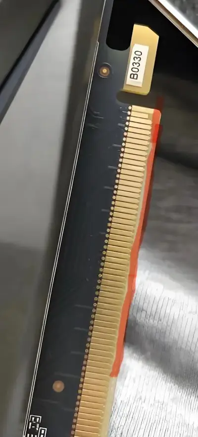
After the first HASL cycle, the pads already contain a solder coating. During a second exposure to molten solder and hot-air leveling, the existing solder layer may remelt and redistribute across the pad. Therefore, a second HASL process does not necessarily double the solder thickness. Instead, it may produce localized increases in solder volume, differences in pad height, or changes in surface flatness.
The impact may be limited on large pads with relatively generous spacing. However, fine-pitch ICs, QFN packages, BGAs, and fine-pitch connectors are much more sensitive to pad height and coplanarity. Changes in the pad surface can affect the contact between the PCB and the solder paste stencil. This may lead to uneven solder paste transfer and increase the risk of solder bridges, insufficient solder, or open joints during reflow.
Pad coplanarity is especially important when several adjacent pads must receive a consistent solder paste volume. A locally raised area can alter the stencil-to-board gap, while an uneven solder surface can cause some pads to receive more paste and others to receive less. The resulting defect pattern may not be obvious from a visual inspection of the bare board.
2. Increased Thermal History
HASL finish is already a high-temperature manufacturing process. A second HASL cycle exposes the PCB to another thermal excursion. A PCB consists of copper foil, glass fiber, resin, and solder mask, and these materials do not have identical thermal expansion characteristics. Repeated heating and cooling can therefore increase residual stress within the board.
This effect is more significant for large-format boards, thick boards, multilayer boards, PCBs with large copper areas, and high-layer-count constructions. Possible consequences include board warpage, bow and twist, dimensional change, or increased localized stress between layers. These changes may later affect stencil printing, component placement, and the board's ability to remain stable during SMT assembly.
Thermal history should not be evaluated only by counting process passes. The actual impact also depends on the PCB construction and the condition of the board before rework. A board that was already close to its allowable flatness or dimensional limits may have less remaining process margin than a smaller, lower-density board.
3. Effects on the Solder Mask and Pad Interface
During a second HASL cycle, the solder mask is exposed again to high temperature and thermal shock. If the original solder mask process or material condition was already near its process limit, repeated heating may increase the risk of discoloration, reduced adhesion, blistering, edge lifting, or localized damage.
The interface between the copper pad and the solder coating must also be considered. Copper and solder can form copper-tin intermetallic compounds at elevated temperature. A first HASL cycle has already produced a certain amount of Cu-Sn IMC, and additional heating may allow this intermetallic layer to grow further.
Under normal process control, a second HASL cycle does not automatically mean that a failure will occur. However, it adds unnecessary thermal exposure and changes the material history of the pad interface. For automotive, industrial, telecommunications, and other high-reliability products, this additional process history should be evaluated rather than accepted solely on the basis of appearance.
4. PTH Reliability
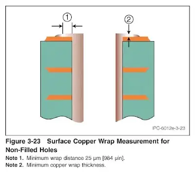
When the PCB contains a large number of through-hole components, the condition of the plated-through holes requires particular attention. During a second HASL cycle, the hole walls and internal solder coverage are exposed to another high-temperature event. Repeated thermal cycling may increase the thermal stress applied to the plated copper in the hole walls.
The concern is more significant for thick boards, small hole diameters, high-aspect-ratio holes, and high-reliability PTH structures. Visual inspection of the board surface cannot fully confirm the condition of the internal copper plating or solder coverage. Depending on the product requirements, cross-section analysis or other applicable reliability verification should be used to confirm that the plated structure remains acceptable.
Potential Effects During SMT and PCBA Assembly
1. Solder Paste Printing
SMT solder paste printing depends heavily on pad coplanarity and surface condition. If the second HASL cycle increases the local solder thickness or creates a larger height difference between pads, the contact condition between the stencil and PCB may change. This directly affects solder paste transfer.
The result may be excessive solder paste on some pads and insufficient paste on others. During reflow, the variation can increase the probability of solder bridges, insufficient solder, and open joints. For this reason, a PCB that has undergone a second HASL cycle should be evaluated with solder paste inspection (SPI). Comparing normal boards with reworked boards can reveal differences in paste height, printed area, and paste volume.
SPI data is particularly useful because the bare-board appearance may not reveal a small but process-significant change in pad height. The comparison should focus on whether the reworked boards show a consistent shift or greater variation in the solder paste printing results.
2. Fine-Pitch, QFN, and BGA Components
Fine-pitch ICs are highly sensitive to pad spacing and solder volume. If the pad height or solder volume increases, the risk of solder bridging may also increase. For QFN packages, the central thermal pad must remain sufficiently flat. Poor coplanarity can cause the component to stand too high, which may affect the surrounding solder joints and the thermal connection between the package and the PCB.
BGA solder joints are located beneath the component and cannot be fully verified through ordinary automated optical inspection. Consistent PCB pad flatness and solder volume are therefore especially important. When necessary, X-ray inspection should be used to evaluate the condition of the BGA solder joints.
The same principle applies to dense connector patterns and other components with closely spaced terminations. Even if the board appears acceptable before assembly, a small change in the pad surface can become a larger process problem when combined with stencil printing variation, component placement, and reflow behavior.
3. A Second HASL Cycle Does Not Automatically Reduce Solderability
The key issue is not simply that the board has been processed twice. The important question is whether the pad condition after the second process is stable, uniform, and suitable for assembly.
If the original HASL problem was caused by copper oxidation, surface contamination, unsuitable flux, or incorrect equipment parameters, simply repeating the HASL process does not guarantee that the root cause has been eliminated. Before approving rework, the PCB manufacturer should identify the actual cause of the original defect and determine whether a second HASL cycle is an appropriate corrective action.
For the assembly operation, acceptance should not be based only on the visual appearance of the PCB. At a minimum, the evaluation should consider pad appearance, solder thickness, pad coplanarity, board bow and twist, solderability, and, where applicable, PTH condition. For high-density or high-reliability products, an SMT trial run may be necessary, followed by review of SPI and AOI results. BGA and QFN joints may also require X-ray inspection.
How to Evaluate a HASL Rework Decision
A practical evaluation should distinguish between the reason for rework and the possible effects of another thermal cycle. Insufficient solder thickness, poor wetting, and abnormal appearance may have different root causes and may not be corrected by the same method. Repeating HASL without identifying the cause can consume additional process margin while leaving the original problem unresolved.
The evaluation should also consider the relationship between the PCB design and the assembly process. A large-pad, low-density board may tolerate small changes in solder distribution more readily than a board containing fine-pitch ICs, QFNs, BGAs, or dense connectors. Similarly, a small, thin board may be less sensitive to thermal distortion than a large multilayer board with extensive copper areas.
Where the product has limited tolerance for solder-volume variation, board warpage, or hidden-joint defects, PCB manufacturing and SMT assembly teams should define the inspection method together. This prevents a board from being released solely because it passes a surface appearance check while its actual assembly behavior remains unverified.
Conclusion
The main risk of a second HASL process is not simply that solder has been applied twice. The greater concern is that the PCB has experienced a second cycle of high temperature, molten solder contact, and hot-air leveling. This may change pad geometry, surface condition, material thermal history, solder mask condition, and PTH structure.
For products with large pads, low component density, and relatively low reliability requirements, a controlled rework process followed by appropriate inspection may not cause a practical functional problem. However, for BGAs, QFNs, fine-pitch components, large multilayer boards, thick boards, and high-reliability products, a second HASL cycle should be treated as a special rework process. The PCB manufacturer and SMT assembly provider should perform a joint risk assessment and verify the result through process data and, when necessary, assembly trials and internal inspection rather than relying on visual appearance alone.