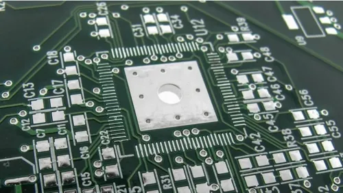
In production we treat the FR4 PCB minimum hole size as a thickness-dependent limit rather than a fixed catalogue number. CAM engineers open the design, measure finished hole diameter against finished board thickness, and calculate aspect ratio first. If the ratio sits outside our standard process window we either enlarge the finished hole or return the file with a clear note on the risk. Most standard FR4 lines run a practical floor of 0.20–0.25 mm finished for 1.6 mm boards; thinner cores can go lower, thicker stacks cannot.
That decision is made before any panel is released to the drill room. We do not wait for the first broken bit to discover the problem.
Why board thickness pushes the hole diameter up on every panel
Drill bits for FR4 are carbide. Once diameter drops below 0.25 mm the flute length-to-diameter ratio climbs fast. On a 1.6 mm panel the bit already works near its stiffness limit; any additional depth or higher glass content raises the chance of deflection or snap. Spindle run-out of 10–15 µm, which is normal on production machines, becomes a large percentage of a 0.15 mm hole and produces oval entry or exit.
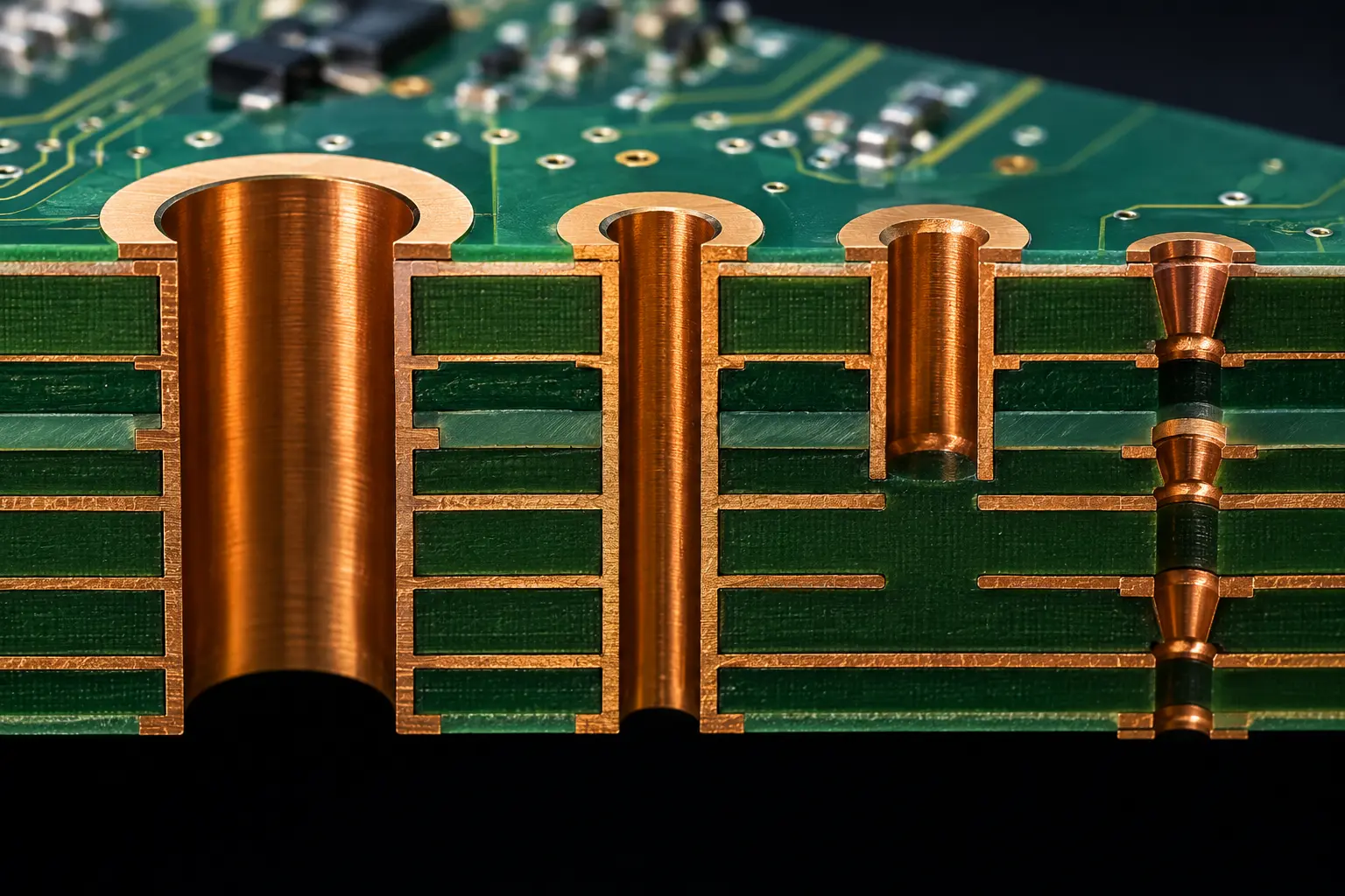
Plating chemistry adds the second constraint. Acid copper must throw into a high-aspect-ratio barrel. Below roughly 8:1 the current density at the centre of the hole falls off, copper thins, and the plating bath leaves voids or thin spots that later crack under thermal cycling. Resin smear from the drill also becomes harder to clean out of a narrow hole, so the desmear step leaves residual material that blocks copper nucleation.
Panelization multiplies the problem. A single panel may contain several hundred small holes. One broken bit stops the whole spindle, forces a tool change, and often leaves a partially drilled panel that must be scrapped or reworked. That is why the FR4 PCB minimum hole size is never judged in isolation from thickness.
What shows up on the floor when the limit is ignored
The first symptom is drill breakage rate climbing above 1–2 % of total hits. Operators start changing bits every few panels instead of every 800–1200 hits. Broken carbide left in the hole is difficult to extract without damaging the pad, so those boards usually go to scrap.
Plating inspection then reveals thin copper or voids mid-barrel. Cross-section samples show copper thickness dropping below 15 µm in the centre while the surface pad is still 25 µm. Those vias pass electrical test at room temperature but open after reflow or thermal shock. Yield loss of 5–8 % on a lot is common when the design sits at the edge of capability.
Routing and solder-mask steps also suffer. Mis-registration of a small hole relative to its pad reduces annular ring to zero on one side, creating breakout that fails AOI. Assembly houses later report intermittent opens or high-resistance vias, which triggers customer returns and schedule slips.

How we actually keep small holes inside process control
CAM first converts finished hole size to drill size by adding the expected plating thickness (usually 0.025–0.040 mm total copper). We then apply a hard aspect-ratio rule: standard FR4 production stays at or below 8:1; advanced lines with better plating throw may accept 10:1 after customer approval. Anything higher is returned with a recommended finished diameter that restores the ratio.
Drill programs for holes under 0.30 mm use reduced chip load, higher spindle speed, and peck cycles to clear chips. Entry and exit material (aluminium or phenolic) is selected to minimise burr and keep the bit straight. Tool life is tracked by hit count; once a bit reaches its limit it is automatically replaced, not pushed further.
Desmear chemistry is adjusted for high-aspect holes—longer dwell or higher permanganate concentration—to clear smear without over-etching the glass. Plating racks are loaded with lower current density and longer time so copper has a chance to build in the centre of the barrel. Final inspection includes coupon microsections on every panel lot that contains holes near the minimum size for FR4 PCB.
When the design cannot be changed we sometimes split the stack: drill the small vias on thinner cores before final lamination, then plate the through-holes separately. That keeps each aspect ratio inside the process window but adds cost and lead time.
When we allow a tighter ratio
Thin boards (0.4–0.8 mm finished) routinely accept 0.15 mm finished holes because the absolute depth is short and plating throw is easier. Prototype lots of fewer than 50 panels sometimes run at 10:1 or 12:1 under special process parameters and 100 % microsection inspection; the customer accepts the higher scrap risk. High-end shops equipped with linear-motor spindles and pulse-plating lines can push the FR4 PCB minimum hole size lower, but those lines cost more and are not the default for volume production.
The trade-off is always the same: tighter holes raise tool cost, slow the drill cycle, and demand tighter process control. If the electrical design can tolerate a 0.05 mm larger finished diameter, most factories prefer that route because yield and delivery stay predictable.
When a design arrives with holes that sit right on the edge of capability we flag it early, show the calculated aspect ratio, and offer the practical options. That conversation happens at DFM review, not after the first panel has already been drilled.