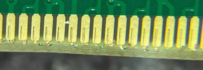
Although palladium is present in PCB production at concentrations measured in micrograms, it can strongly influence the electrical continuity and long-term reliability of an entire board. Palladium does not remain as part of the finished PCB structure in every process. Instead, it acts as a process-critical catalyst in some stages and as a functional barrier layer in others. When its location and concentration are properly controlled, copper deposits densely and pads remain reliable. When even a small amount of palladium is distributed incorrectly, problems such as plating on unwanted areas, incomplete plating, and short circuits can follow.
1. Palladium in Through-Hole Metallization
After PCB drilling, the hole wall consists mainly of electrically insulating resin and glass fibers. Because copper cannot deposit directly onto this nonconductive surface through conventional chemical copper deposition, the hole wall must first be provided with a catalytic seed layer.
This is where colloidal palladium activation is used. The activation solution commonly contains a colloid formed from SnCl2 and PdCl2. Palladium is reduced and deposited onto the hole wall, where it provides the catalytic surface required for electroless copper deposition. The palladium does not serve as the primary conductive layer; its key function is to initiate the chemical reaction that allows copper to grow on the resin and glass-fiber surfaces.
Without sufficient palladium activation, electroless copper may fail to deposit. If the palladium concentration is too low or the activation is incomplete, too few catalytic sites are available during the copper deposition step. The result can be inadequate hole-wall coverage or a complete absence of copper in localized areas, creating an open-circuit defect.
Excessive palladium concentration creates a different type of risk. Palladium ions or palladium-containing residues may remain on non-plated-through holes and on the resin surface of multilayer boards. During a subsequent electroless nickel/gold process, these residual catalytic sites can continue to promote the reduction of nickel ions. Nickel and gold may then deposit on hole walls that should remain nonmetalized, producing unwanted gold on NPTH surfaces.
Consequently, palladium concentration in the activation bath must be controlled between two opposing process limits: insufficient activation, which can cause missing copper, and excessive activation, which can cause unintended deposition. The correct operating window depends on the specific chemistry and process conditions, so palladium concentration should not be treated as an isolated parameter.
2. Residual Palladium and Surface-Finish Defects
After hole metallization, the PCB proceeds through solder mask formation, development, pattern plating, etching, and surface finishing. During solder mask development, side etching or exposed regions around the mask pattern may retain residues from the activation chemistry. If these residues are not completely removed, the remaining palladium can become an unintended catalyst in a later chemical nickel/gold process.
The problem is especially serious when palladium remains in insulating areas between adjacent conductors. Palladium is difficult to dissolve using some conventional etchants, so it may survive the etching stage even after unwanted copper has been removed. During subsequent electroless metal deposition, the residual palladium can continue to catalyze metal growth in areas that are supposed to remain electrically isolated.


When metal deposits bridge the insulating space between traces, the result is plating bleed, insulation failure, or an electrical short. This is why some PCB processes include a dedicated palladium-removal or palladium-passivation step after activation. Chemicals such as sodium sulfide can deactivate or convert residual palladium species, reducing their ability to catalyze further metal deposition. The purpose is to interrupt the abnormal catalytic chain before the board reaches a later surface-finishing stage.
From a process-control perspective, palladium-related defects are not limited to the activation tank. Cleaning efficiency, mask-development conditions, rinsing, etching, and the condition of the non-plated areas all affect whether palladium remains where it should not. A stable process therefore requires control of both palladium application and palladium removal.
3. Palladium as a Functional Layer in ENEPIG
When the selected surface finish is electroless nickel/electroless palladium/immersion gold, or ENEPIG, palladium has a different role. It is no longer used only as a temporary catalyst. Instead, it becomes a defined structural layer between the nickel and gold layers.
The primary purpose of the palladium layer in ENEPIG is to reduce mutual diffusion between nickel and gold. In a conventional electroless nickel/immersion gold finish, nickel can diffuse toward the gold layer during extended storage or repeated reflow exposure. Gold can also penetrate toward the nickel layer. Changes at this interface may contribute to the formation of a brittle, gold-rich region and can reduce solder-joint reliability. This failure mechanism is commonly associated with black pad-type defects.
The palladium layer acts as a diffusion barrier. By placing a dense and continuous palladium film between the nickel and gold, ENEPIG provides better separation of the two layers and helps maintain a more stable interface during thermal and environmental exposure.
However, palladium thickness is a critical process parameter. If the layer is too thin, its ability to act as a diffusion barrier may be insufficient. The process discussion identifies a thickness below 0.05 μm as potentially inadequate. If the layer is too thick, above 0.3 μm, solder wetting and solder-joint formation may be adversely affected, particularly with tin-lead solder systems. These values describe the process limits discussed here and should not be applied as universal requirements to every ENEPIG design or chemistry.
4. The Risk of Palladium Penetration into the Substrate
Improper control of the electroless palladium bath can create another defect mechanism: palladium penetration into the substrate or base material. If palladium is adsorbed by the substrate and is not completely removed before subsequent deposition steps, the residual catalytic material can remain below the intended surface region.
For ABF substrates, discontinuous Pd and Au deposition has been observed at depths of approximately 0.3 to 1.0 μm under the conditions described. The underlying cause is residual adsorbed palladium that has not been fully cleaned away. Once activated palladium exists inside or below the surface, it can promote metal deposition in locations that are not intended to become part of the finished conductive structure.
This creates a difficult process balance. A palladium layer that is too thin may not provide adequate barrier performance, while excessive palladium or uncontrolled penetration may interfere with solderability and create hidden plating defects. The issue is therefore not simply whether palladium is present, but whether it is present at the correct depth, in the correct area, and with a sufficiently uniform distribution.
5. Palladium Distribution Determines PCB Reliability
The two fundamental functions of palladium in PCB manufacturing are catalysis and diffusion blocking. Both functions depend on precise control of position and quantity.
- If palladium remains in an insulating area, it can promote unwanted metal deposition and cause a short circuit.
- If too little palladium is available during activation, copper deposition may fail and create an open circuit.
- If excessive palladium penetrates into the substrate, it can contribute to abnormal internal plating or plating bleed.
- If the catalytic layer is uneven, localized areas may lack sufficient catalytic activity, resulting in incomplete copper coverage or voids.
- If the ENEPIG palladium layer is not continuous, its ability to block nickel-gold diffusion may be reduced.
These failure modes have a common root: uncontrolled palladium distribution. Effective process control must therefore address the complete palladium path, including activation, rinsing, cleaning, deactivation, electroless copper deposition, surface finishing, and final inspection. Concentration control in the chemical bath is necessary, but it is not sufficient by itself. The condition of the substrate, the effectiveness of rinsing, the removal of residues, and the uniformity of the deposited layer all influence the final result.
Palladium may appear to be a minor material in terms of quantity, yet it performs a major role in PCB manufacturing. In through-hole metallization, it provides the catalytic foundation for electroless copper. In surface-finishing processes, residual palladium can trigger unwanted deposition in insulating regions. In ENEPIG, a controlled palladium film serves as a barrier between nickel and gold. Across all these applications, the engineering requirement is the same: palladium must be placed accurately, used at the appropriate level, distributed uniformly, and removed or deactivated wherever it is not required.