In production we treat FPC dimensional change after lamination as a predictable material behavior, not a defect. CAM engineers apply a pre-compensation scale factor to the artwork before the job is released to the press. The scale is derived from the specific PI film type, copper weight, copper coverage percentage, and the measured shrinkage of the previous identical stack-up. Typical compensation falls in the 0.05 % to 0.25 % range in both X and Y; the exact value is locked only after the first panel of a new material lot is measured on the optical coordinate machine.
Residual Stress That Appears The Moment The Press Cools
The root of flexible PCB shrinkage sits in the thermal cycle of the lamination press. Most FPC presses run at 180–200 °C under 20–40 kg/cm² for 60–90 minutes. Polyimide expands freely at that temperature because its in-plane CTE is higher than copper's. When the press cools, the copper layer contracts less than the PI, so the PI is pulled into compression. Once the panel is unloaded, that residual compressive stress relaxes over the next few hours and the panel contracts. The amount of contraction is not uniform; it depends on how much free PI remains between copper features.
We see the largest FPC dimensional change on designs with low copper coverage or large open areas of adhesive-coated PI. High copper density locks the PI in place and reduces the free movement. Uneven copper distribution between top and bottom layers or between left and right halves of the panel produces differential shrinkage that shows up as bow or trapezoidal distortion rather than simple uniform scale change.
What The Panel Looks Like When The Scale Factor Is Ignored
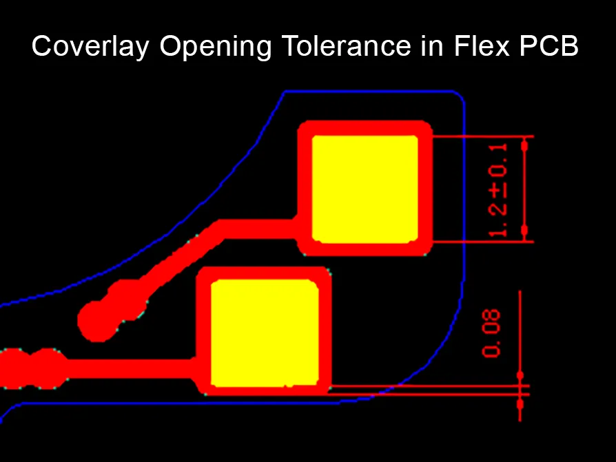
If CAM releases the job at 1:1 and the material shrinks 0.15 %, a 300 mm panel loses 0.45 mm overall. That is enough to push plated through-holes outside the annular-ring tolerance, to misalign coverlay openings relative to pads, and to make the finished outline fail the customer's mechanical drawing. On multi-layer FPC the layer-to-layer registration drifts; subsequent laser or mechanical drilling then hits the wrong location. Yield drops immediately because the parts cannot be salvaged by routing or punching. In high-volume runs the entire lot is scrapped or requires a full re-spin of the artwork, which delays shipment by at least one press cycle plus the time to re-measure.
How CAM And Process Engineers Actually Lock The Dimension
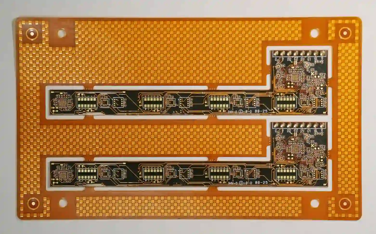
The working method is straightforward. Before the first panel of a new material combination is pressed, CAM calculates an initial scale based on historical data for that PI thickness, copper weight and average copper coverage. After the panel comes out of the press and stabilizes for at least four hours, the coordinate measuring machine records the actual distance between fiducials. The difference between the artwork distance and the measured distance becomes the new scale factor for the remaining panels of that lot. Most factories keep a living table of scale factors indexed by material lot number and copper-coverage bins (0–30 %, 30–60 %, >60 %). When the copper distribution is strongly asymmetric, we apply different X and Y scales or even a local mesh compensation if the CAM system supports it.
Press parameters are also held tight. Ramp rate, peak temperature dwell and cool-down rate are fixed for each stack-up; any deviation changes the residual stress and therefore the final shrinkage. Material incoming inspection includes a quick CTE check on the PI film itself so that a new roll with an outlier CTE can be flagged before it reaches the press. This closed-loop approach keeps flexible PCB shrinkage inside the tolerance window for the majority of production lots.
When The Factory Can Relax The Compensation
For designs with overall tolerance wider than ±0.3 mm or single-layer FPCs with no coverlay registration requirement, we sometimes release at 1:1 and let the customer absorb the small dimensional change. Low-copper rigid-flex sections that are constrained by the rigid portion also need less aggressive scaling. The trade-off is that any subsequent laser drilling or punching must still be programmed from the measured post-lamination data, not from the original artwork. We never skip compensation on multilayer flexible circuits or on parts that go into high-precision connectors.