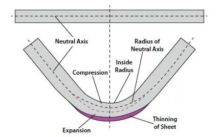
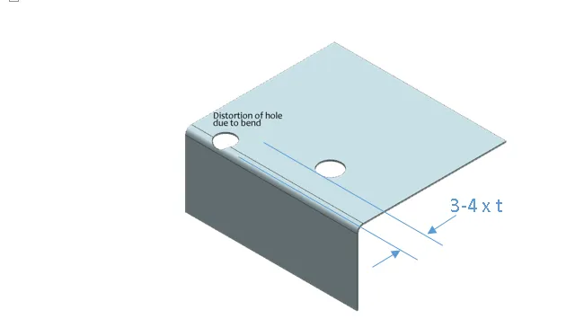
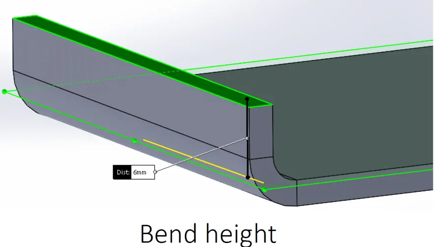
In production we apply process-based default tolerances the moment the flat pattern hits the laser or punch. For mild steel or aluminum in the 0.8–3 mm range the shop standard is ±0.10 mm on linear cut dimensions, ±0.15 mm on hole-to-edge and hole-to-hole positions relative to the flat, and ±1° on bend angles after spring-back compensation. CAM and process engineers override those numbers only when the drawing calls out tighter values and the part can still be held with existing fixtures and gauging. That is the practical sheet metal tolerance design guide we actually run every day.
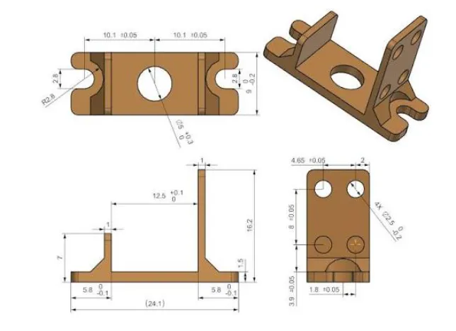
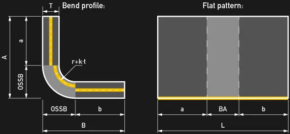
The numbers are not arbitrary. Laser cutters hold better than ±0.05 mm on clean edges when the sheet is flat and the nozzle is fresh, but once the part is nested, clamped and the heat builds up, thermal growth and clamp shift push the practical limit to ±0.10 mm. Punch tools add their own clearance and wear, so the same feature cut on a turret often sits at ±0.15 mm. Bend angles start from the material's measured spring-back; a 90° nominal on 1.5 mm cold-rolled steel usually needs 1.5–2.5° over-bend, and residual variation after that is still ±0.8–1.2°. Hole positions that sit after a bend inherit both the flat tolerance and the angular error multiplied by the flange length, which is why a 50 mm flange with ±1° error already contributes ±0.9 mm of location scatter.
Where material thickness and multi-step sequences push the numbers wider
Thinner gauges amplify every variable. Below 1 mm the sheet flutters under the laser head and spring-back becomes less predictable because grain direction and residual stress dominate. Above 3 mm the punch or laser kerf starts to taper and the press-brake requires higher tonnage, both of which open the process window. When a part carries three or more bends the positional stack-up is no longer additive in a simple arithmetic sense; each bend rotates the previous error vector, so a ±0.2 mm flat error can become ±0.6 mm at the final interface after two 90° folds. That is the real origin of the cumulative-error problem we see on the floor—not designer arithmetic, but sequential process deviation that cannot be zeroed out without intermediate gauging or fixtures that most production runs will not justify.
Equipment capability sets the floor. A well-maintained fiber laser with active following can hold ±0.08 mm day after day on 2 mm steel; the same machine on a warped 4 mm plate or a dull lens drifts to ±0.25 mm. Press-brake back-gauges are typically ±0.05 mm, yet the actual flange length after forming still carries the angular uncertainty. Hole position relative to a bend line is therefore limited by the combined uncertainty of flat location plus the tangent of the angle error times flange length. That combination is why we rarely claim better than ±0.2 mm on critical hole-to-bend features without a secondary drill or mill operation.
What shows up on the shop floor when the drawing is tighter than the process
If the drawing demands ±0.05 mm on a laser-cut outline or ±0.3° on a bend without allowing compensation, the first parts out of the machine already sit outside the band. Operators then either stop the job and call for a process change, or they force the parts through and the CMM rejects them at final inspection. Either path creates scrap or rework: secondary laser trimming, hand filing of flanges, or complete re-blanking. On a 200-piece order that can easily consume an extra shift and push the shipment date. Assembly downstream feels it next—bolt holes that no longer line up, covers that rock, or welded joints that require excessive gap fill. The cost is not only the rejected panels; it is the lost press-brake capacity and the engineering time spent chasing a tolerance the process was never capable of holding.
Cumulative error compounds the damage. A part that looks acceptable after the first bend can walk out of tolerance after the third because each angular deviation is locked in before the next station. Without intermediate checks the final hole pattern can be 1 mm off relative to the mounting face even though every individual feature was cut and bent inside its own local tolerance. That is the classic failure mode we see when designers treat every dimension as independent rather than sequential.
How the production side actually keeps the numbers under control
We start with a process-capability map that is already written into the CAM system. Laser programs default to ±0.10 mm; bend programs apply measured spring-back tables for each material lot and thickness. When a drawing calls for tighter values we first check whether the feature can be held by changing the sequence—cutting critical holes after the last bend, or adding a simple locating pin fixture on the brake. If that still falls short we quote a secondary operation (CNC mill, jig drill, or selective grind) and the associated cost. For hole-to-bend relationships we routinely apply a 0.3–0.5 mm positional buffer in the flat pattern so that the final formed location lands inside the assembly tolerance.
Material thickness is treated as a process variable, not a fixed number. Incoming coil or sheet is measured; if it sits at the high end of the commercial tolerance the spring-back compensation is adjusted upward before the first part is bent. Grain direction is noted on the nesting layout for parts that require consistent flange length. Cumulative stack-up is managed by identifying the primary datum early and measuring every subsequent bend relative to that datum rather than to the previous flange. In practice that means a simple go/no-go gauge or a laser tracker check after the second bend on any job that has three or more critical interfaces.
The same discipline applies to cost control. Overly tight call-outs force either special tooling or 100 % inspection. Both raise the piece price. When the drawing uses the shop-standard ranges listed above, the part runs on standard nests, standard dies and standard cycle times. That is the single most effective way to keep the cost down while still delivering a functional assembly.
Where the factory will accept a looser band without argument
Non-functional edges, cosmetic flanges that never mate, and internal cut-outs that only clear a cable are routinely allowed to float to ±0.3 mm or ±2°. Prototype or low-volume runs can also carry wider numbers if the customer accepts that the first articles will be used to dial in the compensation rather than to prove absolute capability. When the part is welded into a larger assembly the weld gap itself often absorbs ±0.5 mm of variation, so we will relax the preceding features accordingly. The trade-off is always the same: tighter numbers buy better interchangeability at the price of longer lead time and higher unit cost; looser numbers buy speed and lower cost at the price of possible selective assembly or minor fitting at the customer's floor.
In short, the workable sheet metal tolerance design guide is the one that matches the real capability of the laser, the brake and the material lot sitting on the floor that day. Anything tighter requires an explicit process plan and a cost adder; anything looser simply runs.