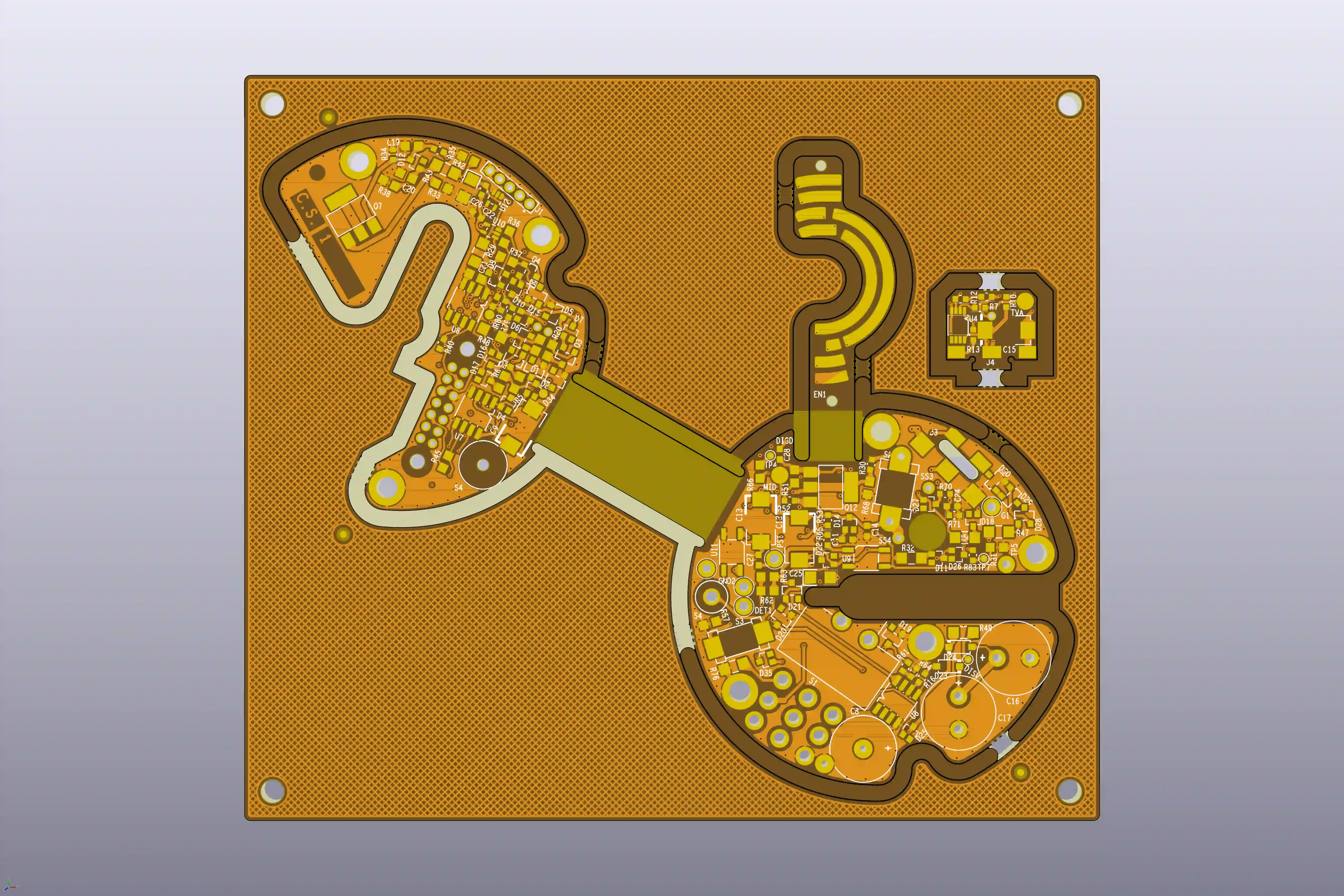
Hybrid Stackup
Hybrid stackup refers to the strategic layering of materials in printed circuit boards (PCBs) that combines different dielectric materials, core types, or even rigid and flexible substrates within a single design. This approach is essential for modern electronics where high-speed signals, thermal management, and mechanical flexibility demand more than traditional uniform stackups. Engineers and designers often turn to hybrid stackup to optimize performance in applications like telecommunications, automotive systems, and consumer devices, where balancing signal integrity, impedance control, and cost efficiency is critical. Understanding hybrid stackup begins with selecting compatible materials that address specific challenges. For instance, integrating low-loss dielectrics for high-frequency layers alongside standard FR-4 for power planes can minimize signal attenuation while maintaining structural integrity. Practical applications include multilayer boards for 5G antennas, where hybrid configurations reduce crosstalk and improve electromagnetic compatibility. Best practices involve careful simulation using tools like Ansys or Altium to predict layer interactions, ensuring controlled impedance and minimal warpage during fabrication. Designers should also consider via structures and prepreg choices to avoid delamination risks, especially in high-reliability environments. For those seeking to implement hybrid stackup in their projects, reviewing detailed case studies and design guidelines can provide valuable insights. Articles tagged under this category delve into real-world examples, from optimizing stackups for RF circuits to troubleshooting common manufacturing issues. By exploring these resources, you can gain the knowledge needed to enhance your PCB designs and achieve superior performance outcomes.
Technical Articles
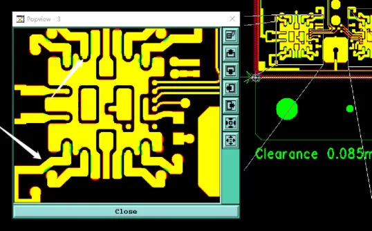
How We Resolved Stackup Warpage, Blind Via Spacing & No-Mask Conflicts in Hybrid Rogers RF PCB
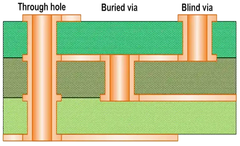
Cost Effective Buried Via Implementation: Balancing Performance and Price

Cost Effective Strategies for High Speed PCB Manufacturing: Balancing Performance and Budget
Short Range Wireless PCB Design for Bluetooth WiFi and Zigbee
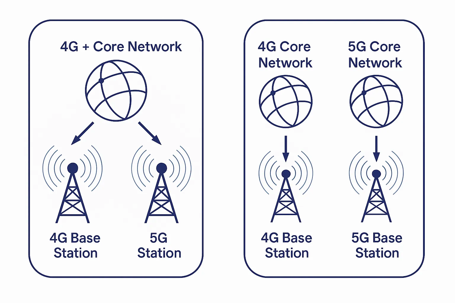
Advanced 5G Technologies: Network Slicing, RedCap, VoNR, and PCB Design Requirements for High-Performance Implementation
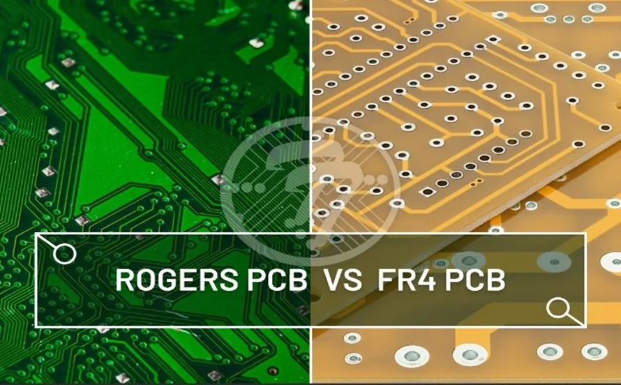
Beyond FR-4: Exploring Advanced Rogers PCB Materials for High-Frequency Applications
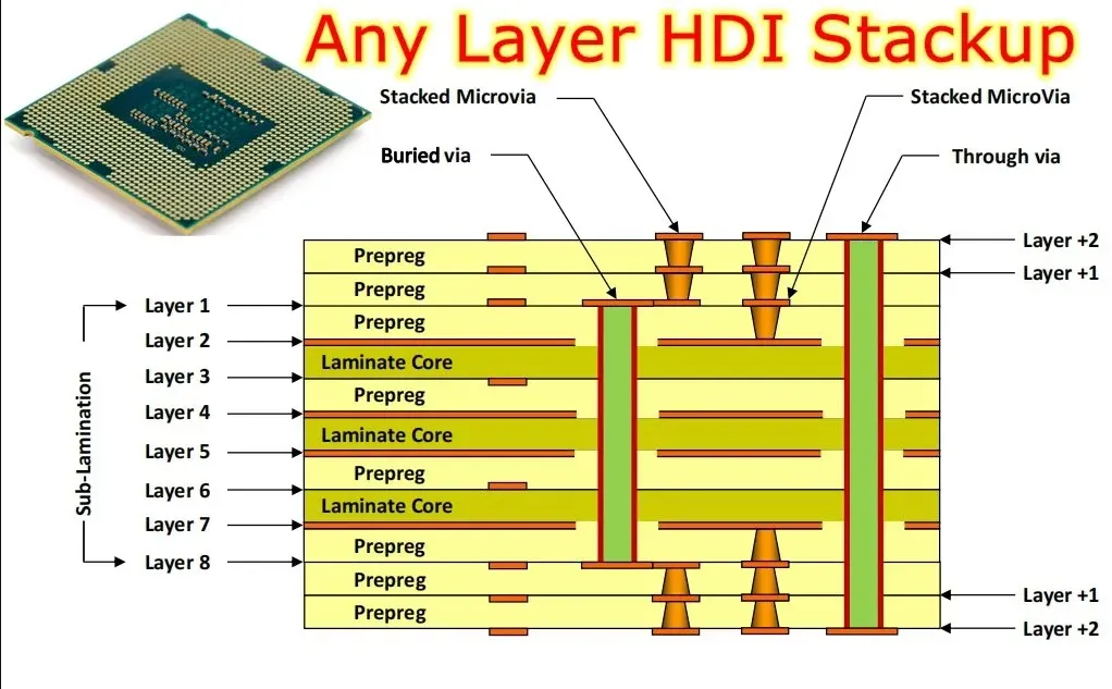
PCB Stack Up to Plan, Design, Manufacture and Repeat

Overview of PLC Ethernet Open Communication
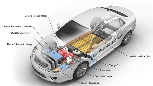
High-Voltage PCB Design for Electric Vehicles: 800V Platforms, Battery Management, and Power Distribution Systems
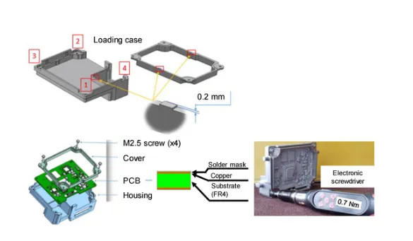
Advanced Techniques for Hybrid Stack Up Design in RF Laminate PCBs
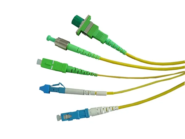
Advanced PCB Design Strategies for Fiber Optic Modules and LiFi Wireless Communication Systems
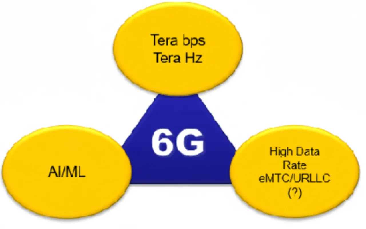
6G Mobile Communications: PCB Design, 3D Integration, and Manufacturing Challenges for THz, AI-Native, and Massive MIMO Systems
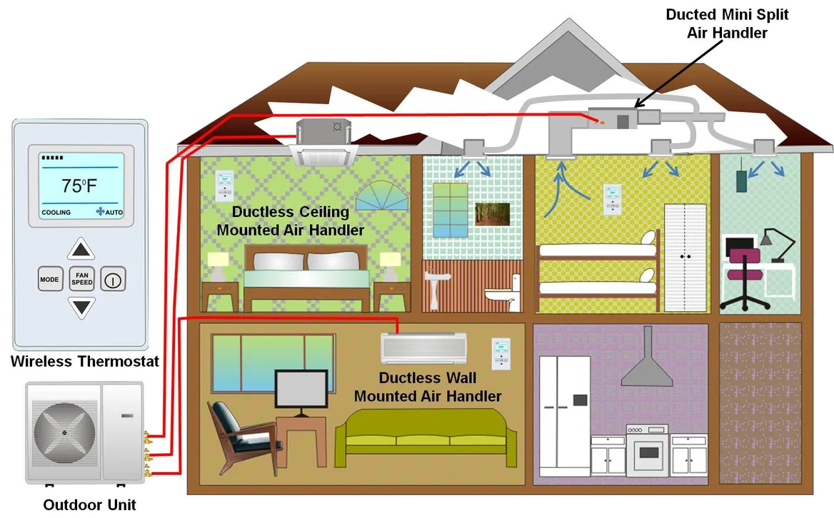
Thermal Management Systems in Electric Vehicles: PCB Design for Heat Pump HVAC, Energy Recovery, and High-Efficiency Control
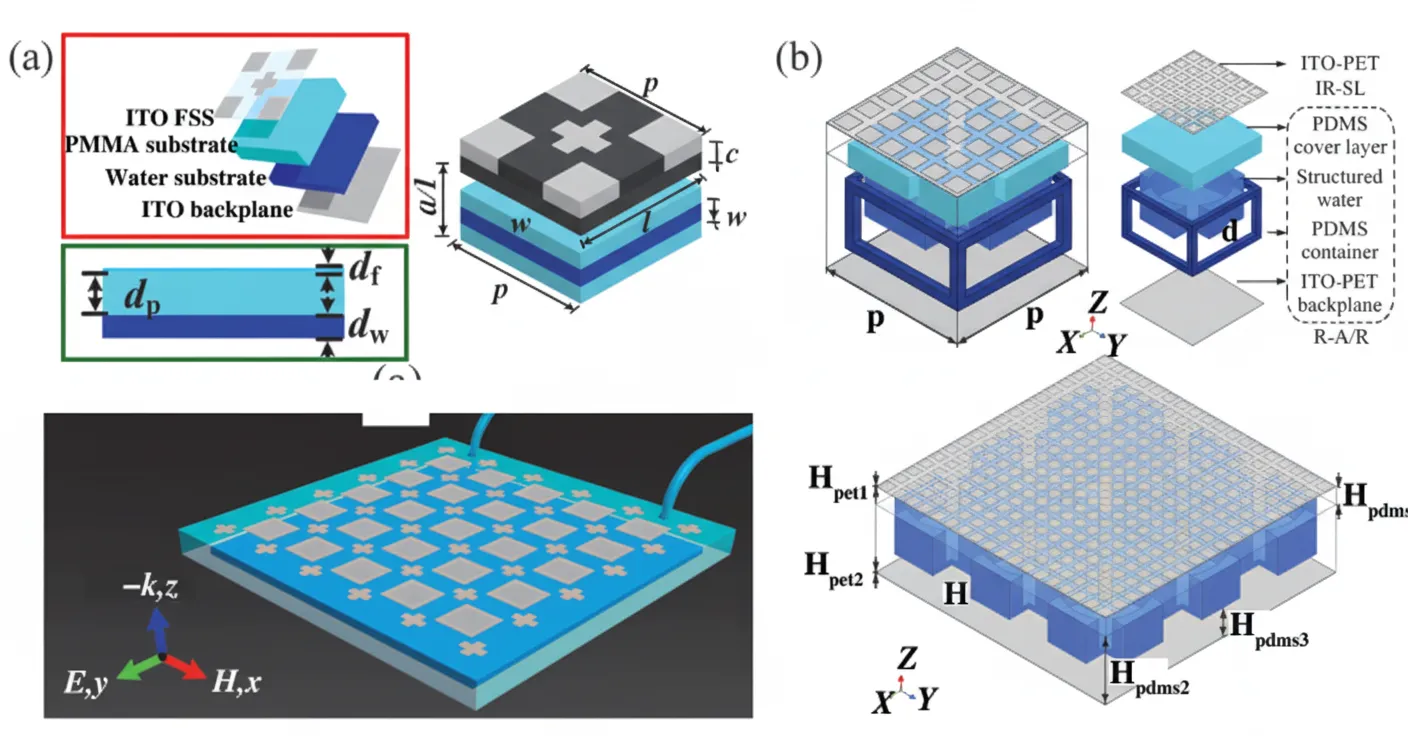
Metamaterial-Enhanced PCBs for RF Stealth, Infrared Compatibility, and Advanced High-Frequency Applications

5G mmWave vs Sub-6GHz: PCB Design Challenges, Material Selection, and Manufacturing Strategies for Dual-Frequency Networks
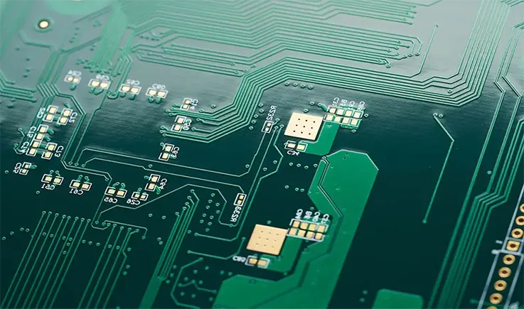
Cost Effective High Frequency PCB Design: Balancing Performance and Price with Taconic Materials
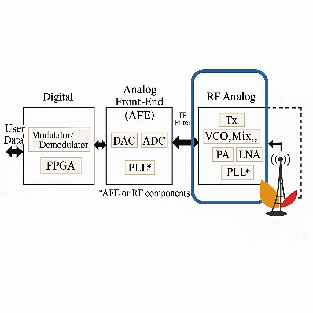
Millimeter-wave Beamforming Systems for Mobile Communications
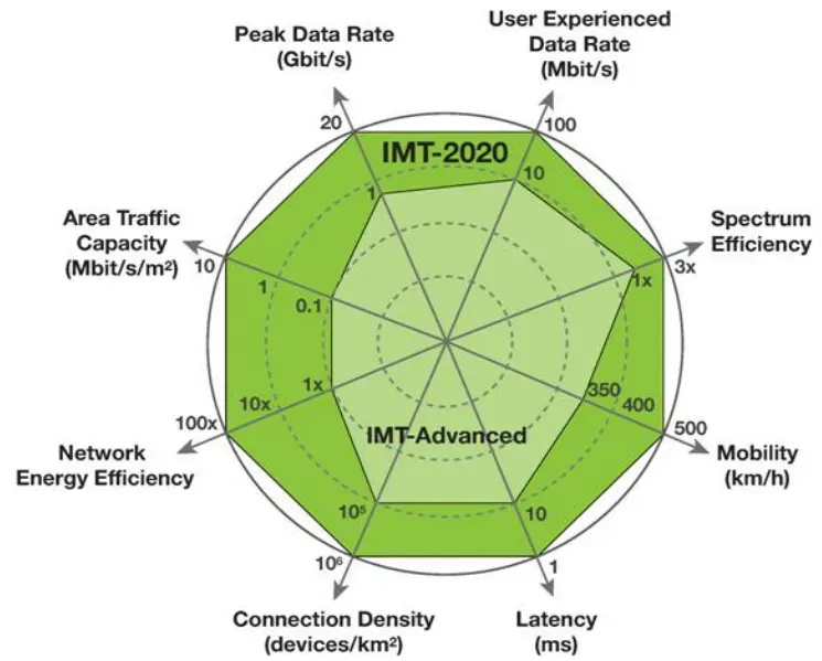
Low Latency in 5G Networks: PCB Design Strategies for Reliable Handovers, Voice Performance, and User Experience
Rogers PCB Application: The Strategic Guide to High-Frequency and High-Speed Design
Get in Touch
Send Message
- Products & Service
- Company
- About AIVON
- Contact
- News
- Blog
- Certification
-


- Payment
-


2026 AIVON.COM All Rights Reserved