 00:58
00:58
PCB Design Rules
PCB design rules form the foundational guidelines that ensure printed circuit boards function reliably, meet manufacturing standards, and perform optimally in real-world applications. These rules encompass a wide range of considerations, from trace width and spacing to via placement, layer stacking, and signal integrity. For engineers, hobbyists, and professionals searching for PCB Design Rules, this tag serves as a comprehensive resource to navigate the complexities of board layout, helping you avoid costly errors like electromagnetic interference, thermal hotspots, or fabrication failures. Understanding and applying these rules is crucial for creating efficient designs that comply with industry standards such as IPC-2221 or specific requirements for high-speed circuits. Practical applications include optimizing power distribution in consumer electronics, ensuring robustness in automotive systems, or enhancing performance in aerospace components. By adhering to best practices, such as maintaining minimum clearances to prevent short circuits or incorporating ground planes for noise reduction, designers can achieve higher yields and longer product lifespans. The articles gathered here offer actionable insights, including step-by-step checklists for rule checking in software tools like Altium or Eagle, case studies on troubleshooting common violations, and tips for adapting rules to advanced technologies like flexible PCBs or high-frequency designs. Whether you are refining a prototype or scaling up for production, these resources provide the knowledge to implement effective strategies tailored to your project's needs. Readers often find value in cross-referencing related topics, such as component placement guidelines or DFM principles, to build a more holistic approach to PCB development.
Video Guide

Technical Articles

PCB Hole and Slot Tolerance Conflicts: CAM Cases from Production

How PCB CAM Balances Copper Thickness, Trace Spacing, and Impedance Requirements

The Nine Stages of Analog Circuit Design
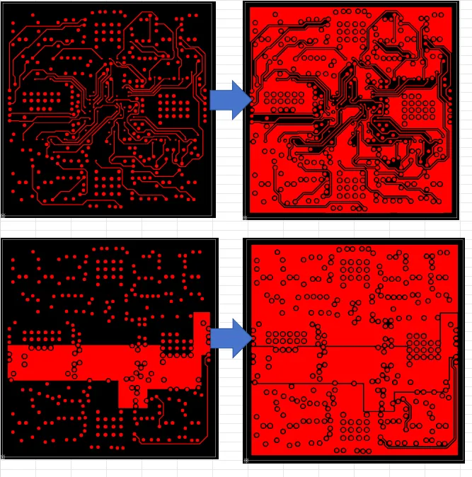
13 Common PCB Design Mistakes—and How to Avoid Them
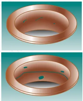
DFM Manufacturability Checks and Recommendations for PCBs

PCIe 7.0 at 128 GT/s: PCB Difficulty Isn’t Just “Shorter Traces”

Cadence Allegro PCB Multi?Trace Routing and Spacing Control
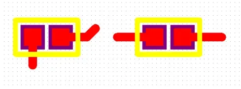
Practical Pad Naming Conventions in PCB Layout Libraries
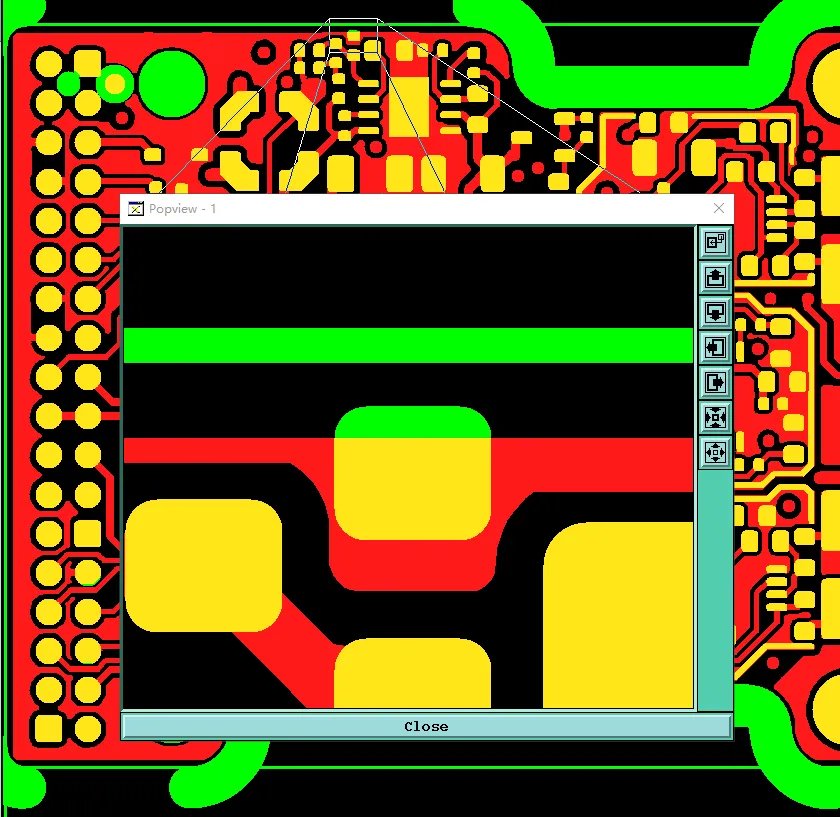
PCB CAM Review for Copper and SMD Pads Near the Board Edge
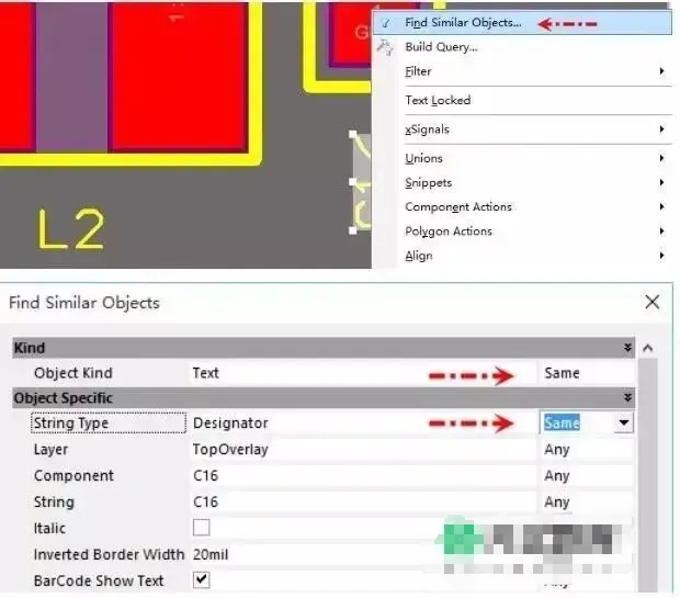
Global Editing Techniques in Altium Designer (Find Similar Objects)
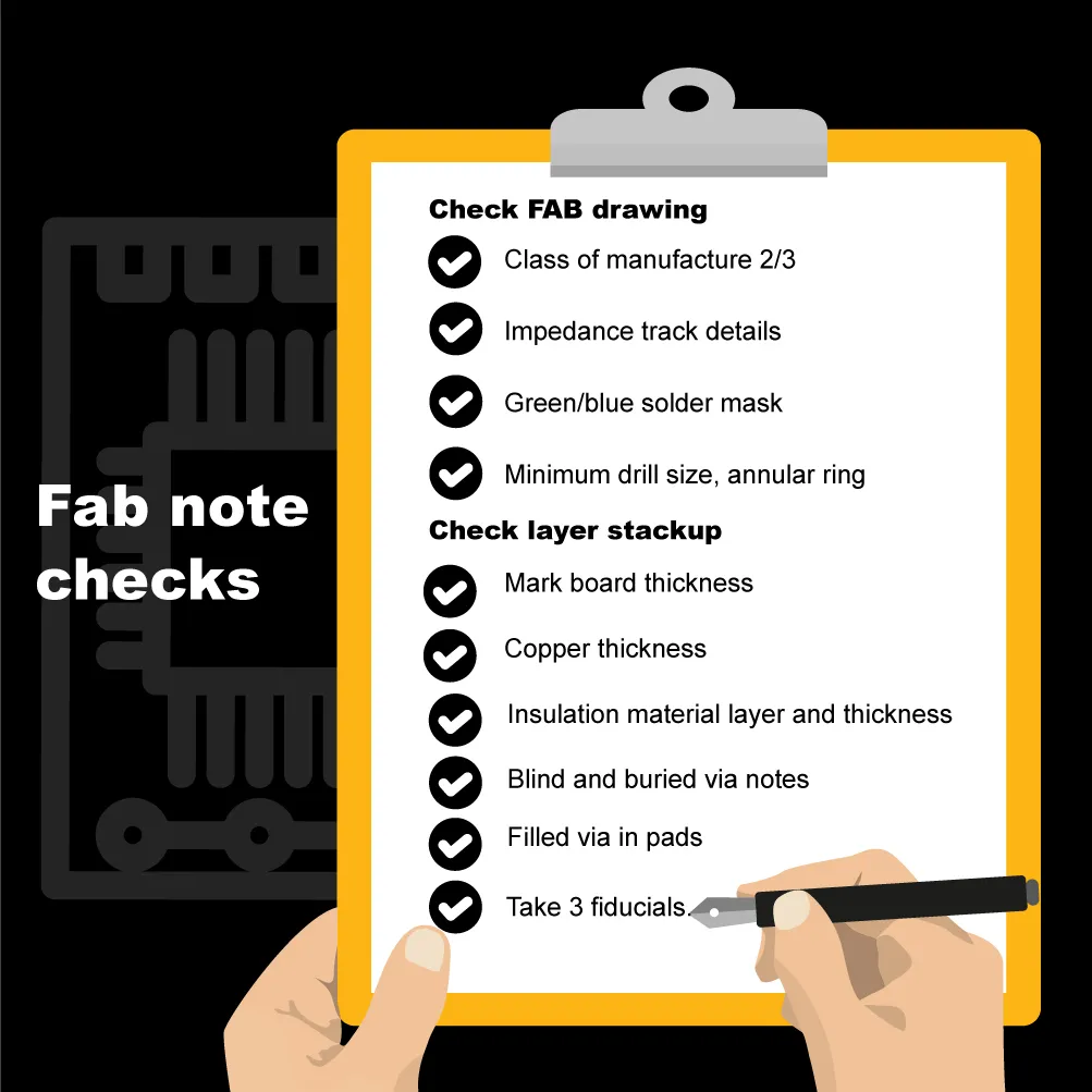
PCB Design Checklist: Design Inputs, Templates, Clock Placement, and Mechanical Controls
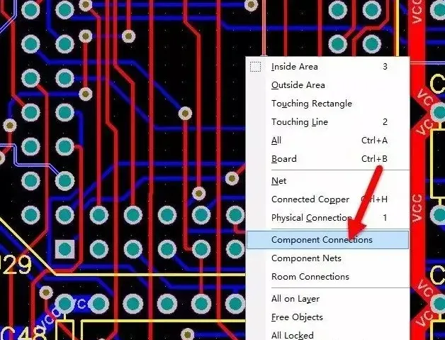
Selecting and Unrouting Nets Associated with a Component in PCB Layout

Common PCB Design Pitfalls and How to Avoid Them

Precise Spacing Control: How to Move a Diagonal Feature by Exactly 1 mm
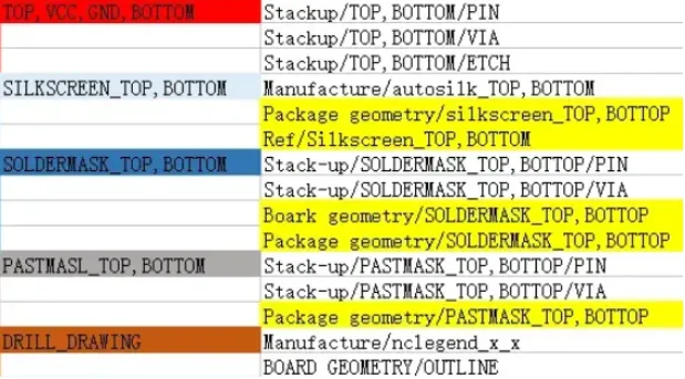
Altium Designer Q&A: Import/Export Rules, Single-Sided PCB Setup, Via Stitching, and Practical Workflow Tips

Do Gerber File Extensions Have Any Special Meaning?

Defining and Using Differential Pairs in KiCad
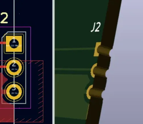
Designing PCB Castellated Holes with KiCad
PCB Layout Design Essentials and Practical Techniques