 00:58
00:58
PCB Design Rules
PCB design rules form the foundational guidelines that ensure printed circuit boards function reliably, meet manufacturing standards, and perform optimally in real-world applications. These rules encompass a wide range of considerations, from trace width and spacing to via placement, layer stacking, and signal integrity. For engineers, hobbyists, and professionals searching for PCB Design Rules, this tag serves as a comprehensive resource to navigate the complexities of board layout, helping you avoid costly errors like electromagnetic interference, thermal hotspots, or fabrication failures. Understanding and applying these rules is crucial for creating efficient designs that comply with industry standards such as IPC-2221 or specific requirements for high-speed circuits. Practical applications include optimizing power distribution in consumer electronics, ensuring robustness in automotive systems, or enhancing performance in aerospace components. By adhering to best practices, such as maintaining minimum clearances to prevent short circuits or incorporating ground planes for noise reduction, designers can achieve higher yields and longer product lifespans. The articles gathered here offer actionable insights, including step-by-step checklists for rule checking in software tools like Altium or Eagle, case studies on troubleshooting common violations, and tips for adapting rules to advanced technologies like flexible PCBs or high-frequency designs. Whether you are refining a prototype or scaling up for production, these resources provide the knowledge to implement effective strategies tailored to your project's needs. Readers often find value in cross-referencing related topics, such as component placement guidelines or DFM principles, to build a more holistic approach to PCB development.
Video Guide

Technical Articles
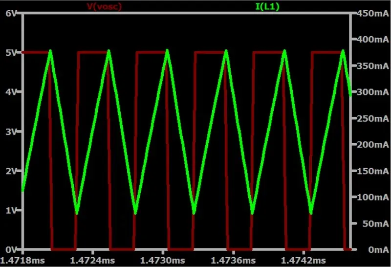
High Output Ripple in Buck DC-DC Regulator: Circuit Analysis
Switching Power Supply PCB Layout Optimization
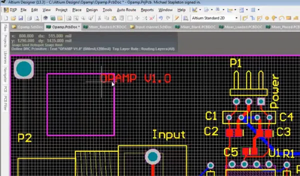
Component Placement: How to use Altium Designer for Perfect PCB Layout
How PCB CAM Review Resolves Copper Weight and Panelization EQs on 8-Layer HDI Boards

Engineering Case Study: 8-Layer FR-4 PCB DFM Clearance Optimization and Resin Plug Hole Confirmation
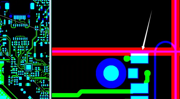
4-Layer FR-4 PCB CAM Review Case: Addressing Via Tenting Conflicts, Routing Layer Discrepancies, and V-CUT Edge Clearance Risks
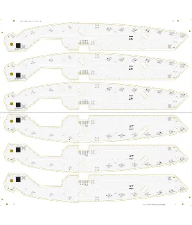
How to Fix SMD Edge Clearance, V-CUT Legend, and Gold Finger Issues in Class 3 PCB CAM Review
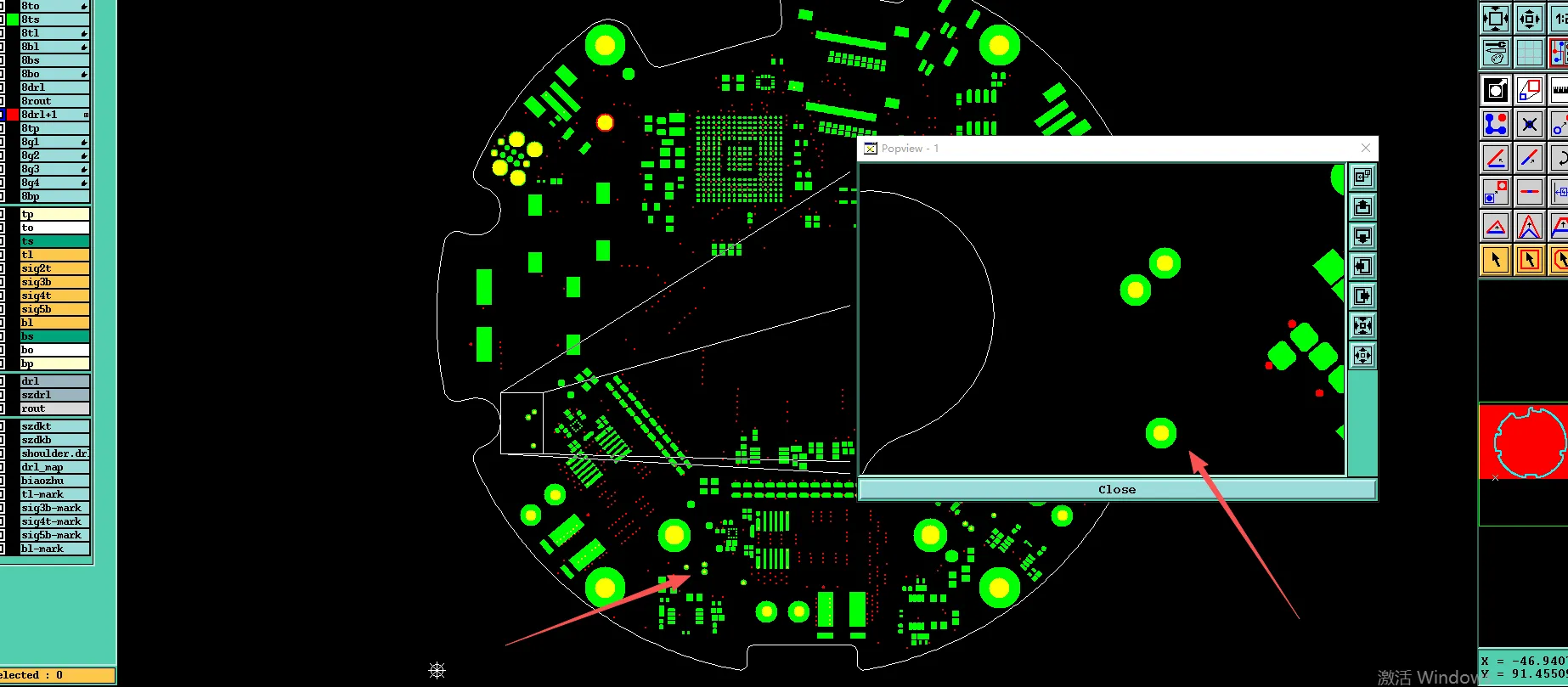
Avoiding DFM Delays: A Guide to PCB Resin Filled Via Design
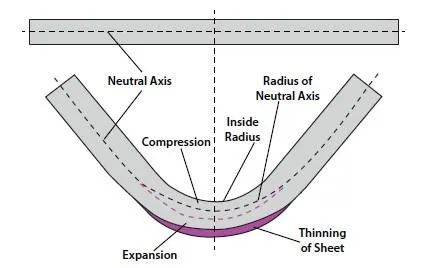
K-Factor vs Bend Allowance in Sheet Metal: What's the Difference?
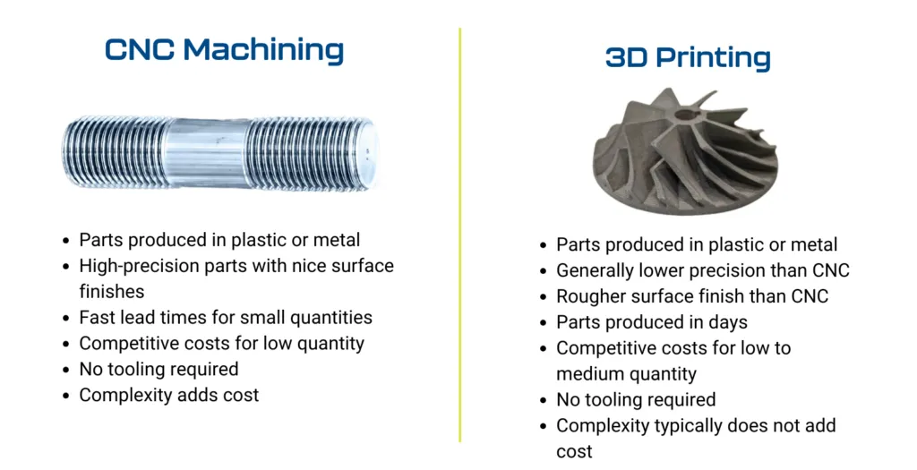
CNC Machining vs 3D Printing Design Rules: What Engineers Should Know
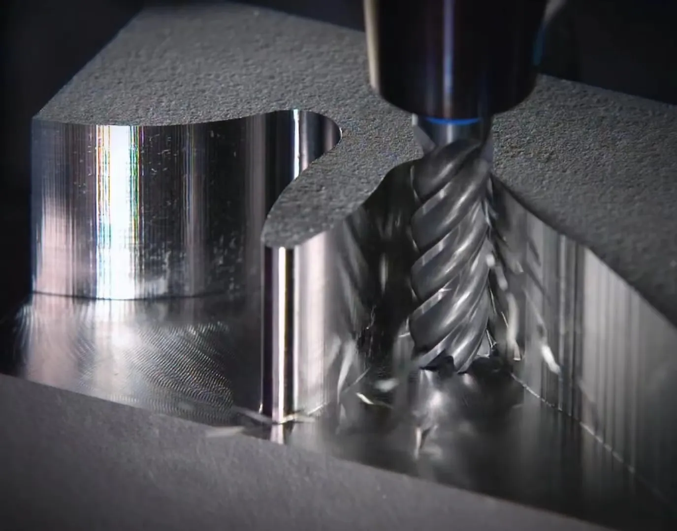
Internal Corner Radius Design Guidelines for CNC Parts
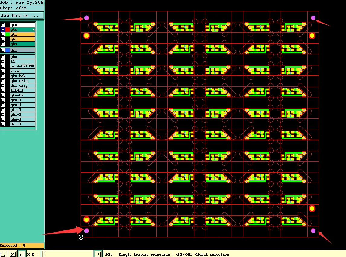
Tented Via vs Open Via Conflict Resolved in 2-Layer FR4 PCB

CNC Machining Wall Thickness Guidelines: How Thin Can You Machine?
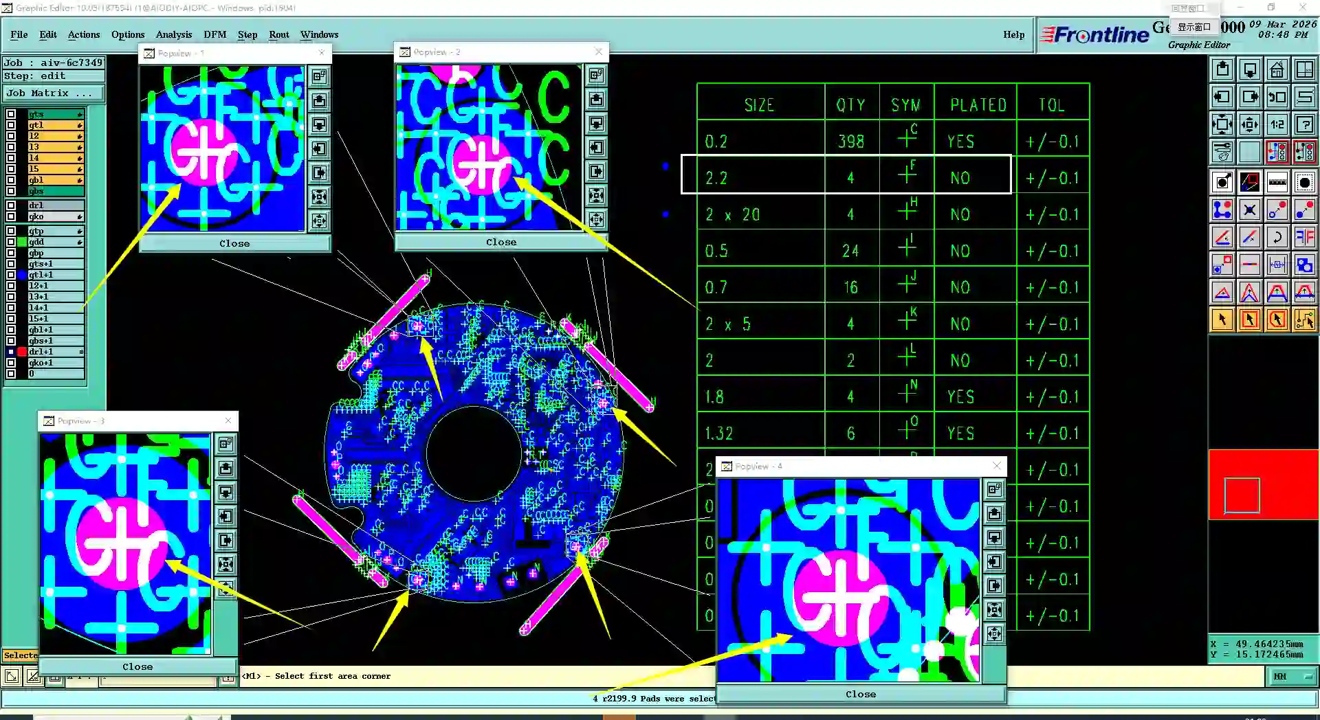
Why NPTH Hole with Pad Conflict Required Clarification Before 6-Layer Production
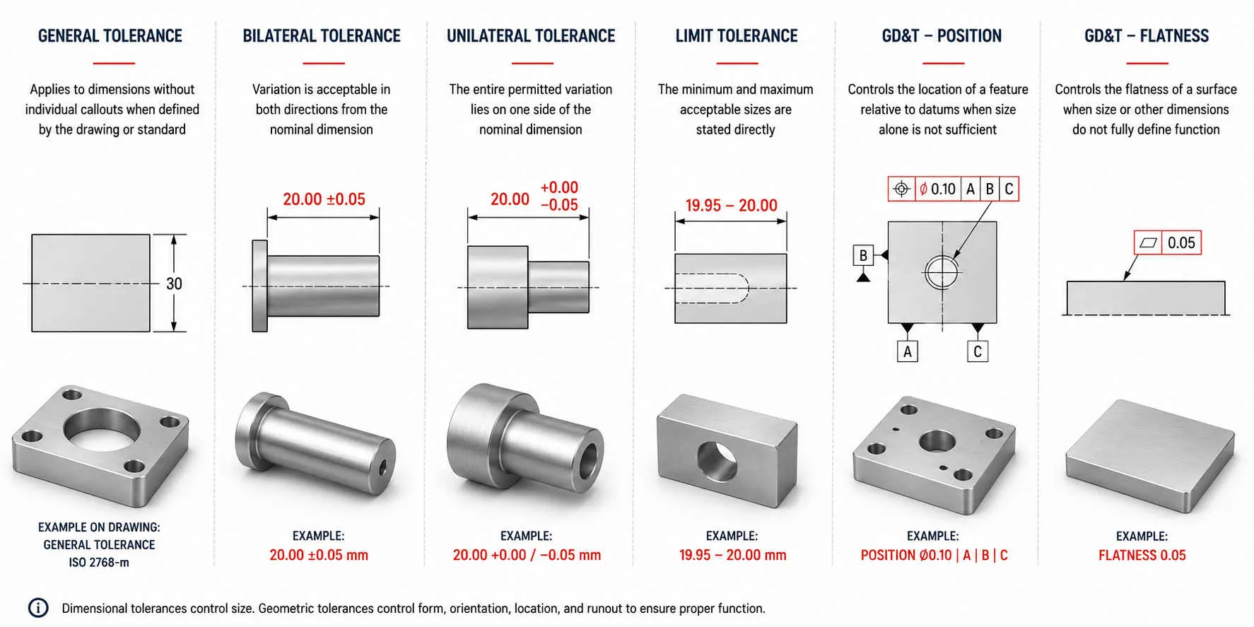
Hole Design Guidelines for CNC Machining
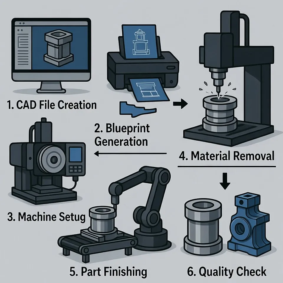
CNC Machining Process Explained: From CAD File to Finished Part
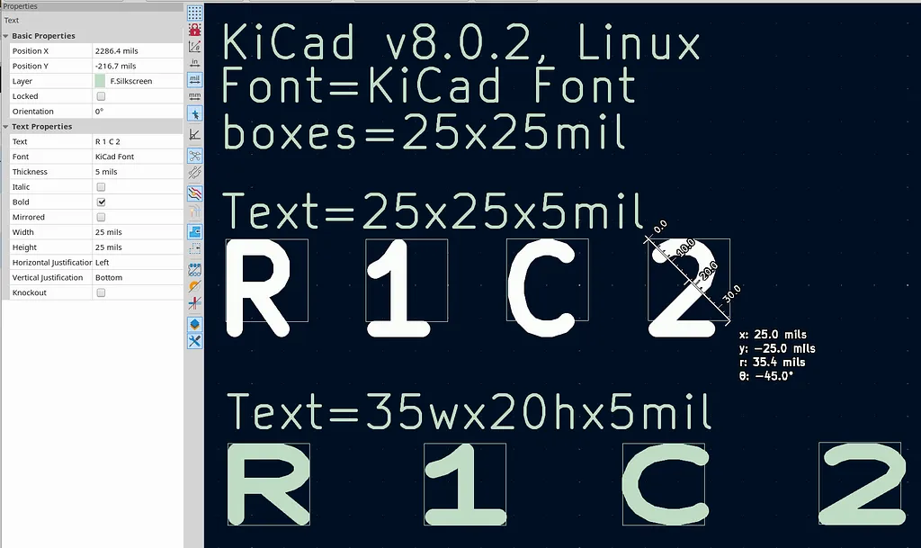
How Small Is Too Small for FPC Legend Text?
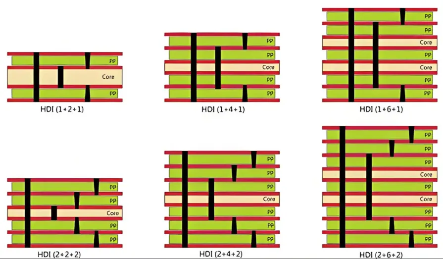
HDI PCB Microvia: A Comprehensive Guide to Design, Reliability, and Manufacturing
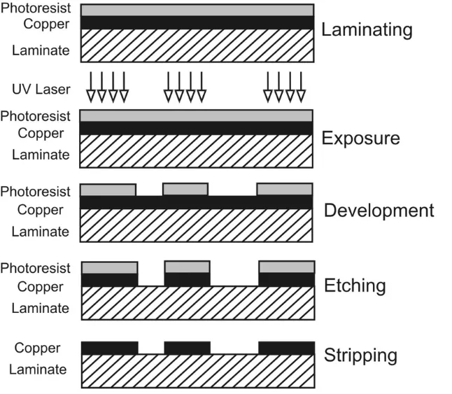
PCB Direct Imaging for Fine Line PCBs: A Comprehensive Guide