 00:40
PCB Fabrication
Printed Circuit Board (PCB) fabrication is a critical process in electronics design and manufacturing, transforming conceptual schematics into functional hardware. This tag page aggregates articles and resources dedicated to PCB fabrication, offering in-depth coverage of the techniques, materials, and workflows involved in producing high-quality circuit boards. Whether you are an electronics engineer prototyping a new device, a hobbyist building custom gadgets, or a manufacturer scaling production, understanding PCB fabrication ensures reliable performance and cost efficiency. Key aspects explored under this tag include the selection of substrate materials like FR-4 or flexible polymers, etching methods such as chemical or laser processes, and layering techniques for multi-layer boards. Readers can find practical guidance on optimizing designs for manufacturability, avoiding common pitfalls like signal integrity issues or thermal management failures, and adhering to industry standards such as IPC guidelines. For instance, articles detail best practices for trace routing, solder mask application, and surface finish options, helping you achieve prototypes that transition smoothly to mass production. By delving into these resources, you gain actionable insights into emerging trends like high-density interconnects and additive manufacturing, which can enhance your projects' innovation and reliability. This collection serves as a valuable reference for troubleshooting fabrication challenges and implementing efficient assembly strategies, ultimately supporting your goals in creating robust electronic systems.
Video Guide
-
00:40
Technical Articles
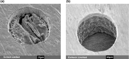
Optimizing Laser Drilling Parameters: A Deep Dive into Power, Frequency, and Speed
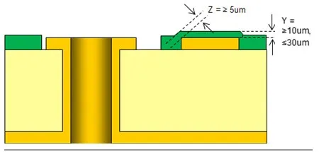
The Ultimate Copper Thickness (Mils) Conversion Chart for PCB Design
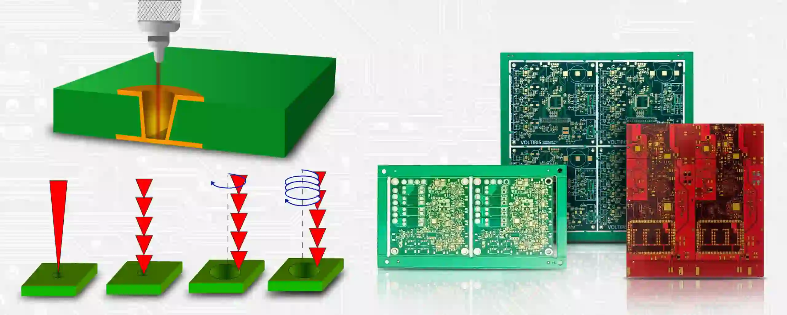
Manufacturing Heavy Copper PCBs: A Step by Step Guide
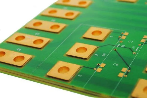
Manufacturing Challenges and Solutions for 3 oz Copper PCBs

The Impact of Solder Mask on PCB Gold Finger Performance: Best Practices

Will QLC All-Flash Replace Hybrid Storage?

Structure Analysis of Stacked DRAM Storage Nodes

Pressure Measurement and Calibration in PCB Lamination and Manufacturing Processes
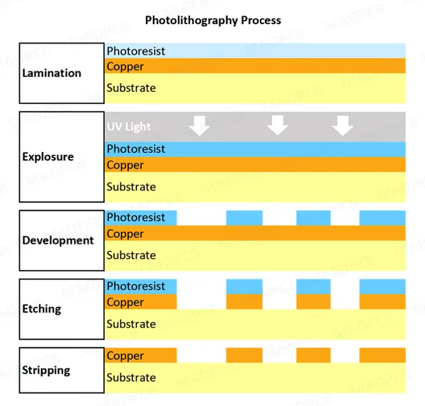
PCB Direct Imaging: Overcoming Challenges with Warped or Uneven Substrates
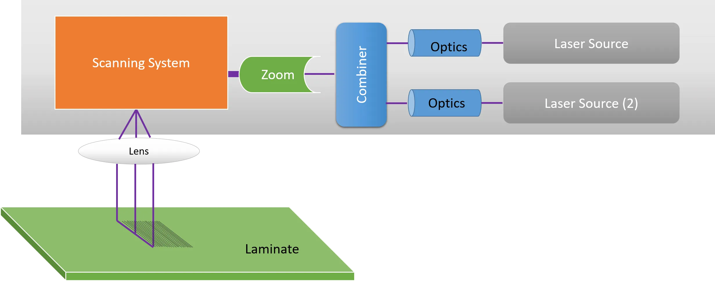
Automating PCB Direct Imaging: Integrating LDI into Your Production Line
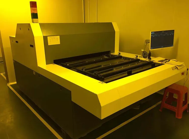
PCB Direct Imaging for High Reliability Applications: Aerospace and Medical
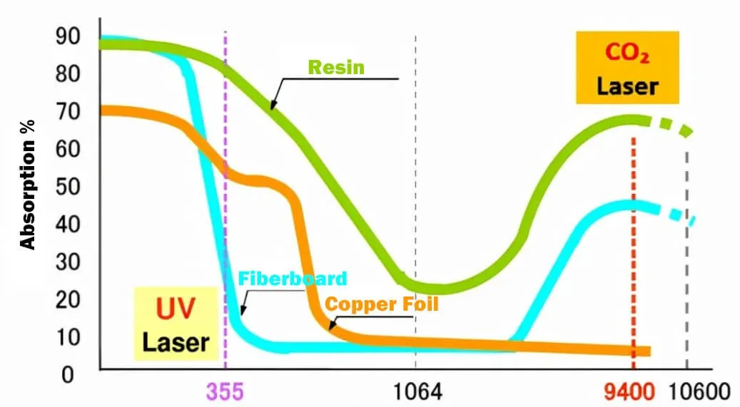
HDI PCB Laser Drilling: Materials, Techniques, and Equipment
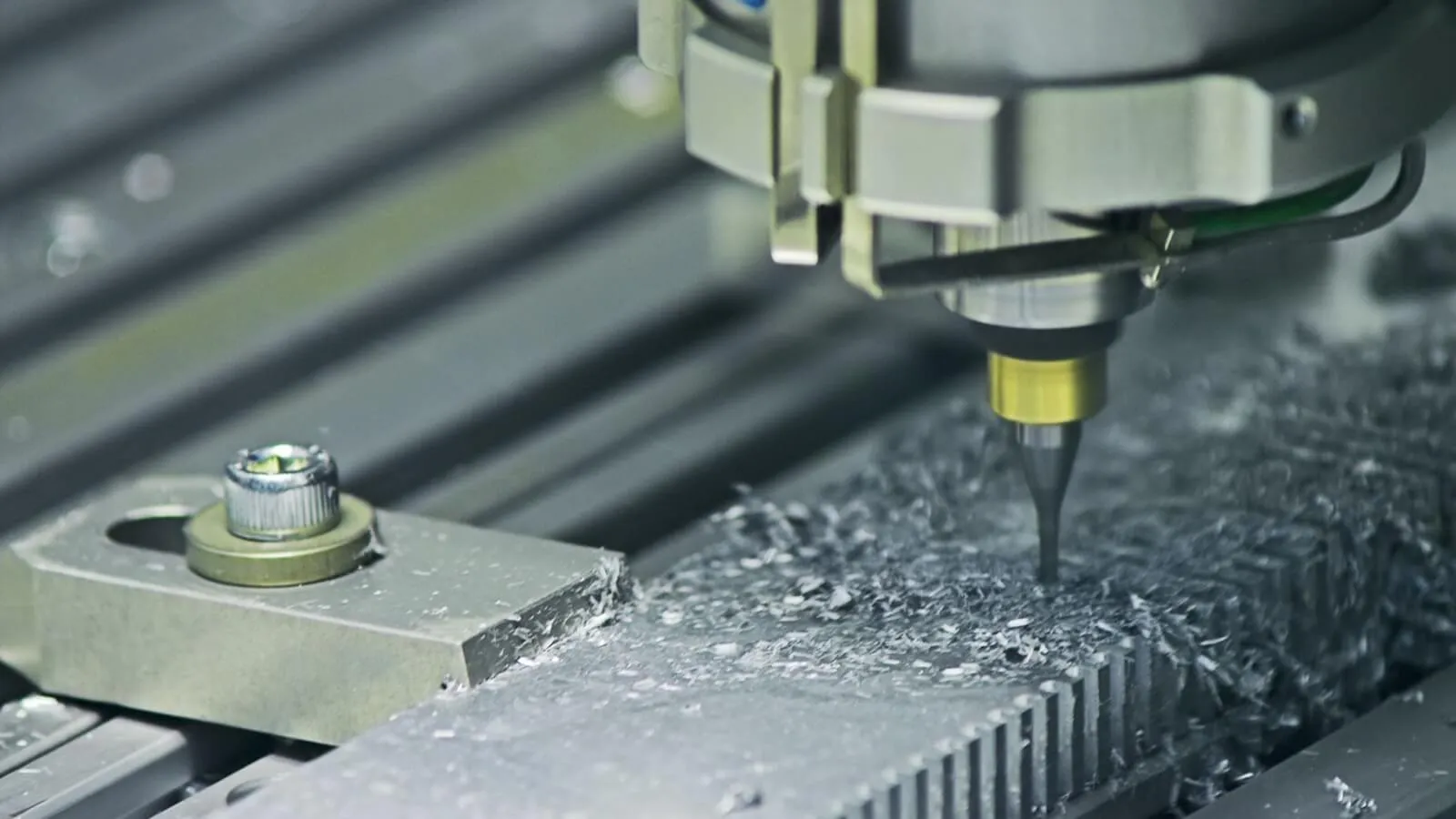
Laser vs. Mechanical Drilling: Which is Better for Your PCB Project?
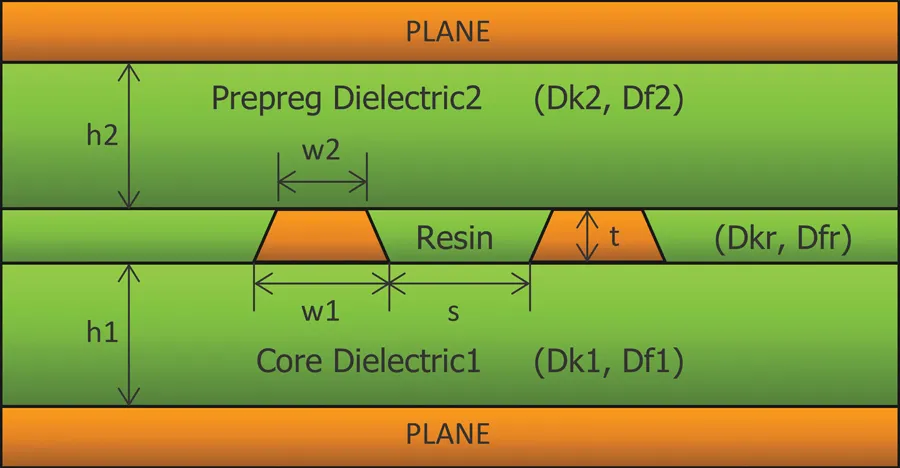
Copper Thickness in Mils and PCB Manufacturing Tolerances: What You Need to Know
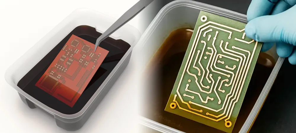
Heavy Copper vs. Standard PCB: Choosing the Right Board
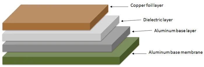
Step by Step: Aluminum PCB Manufacturing Process Explained
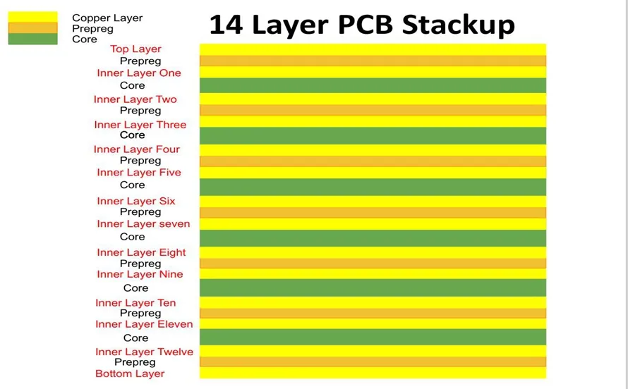
Sequential Lamination for RF and Microwave PCBs: Optimizing Performance in High Frequency Applications
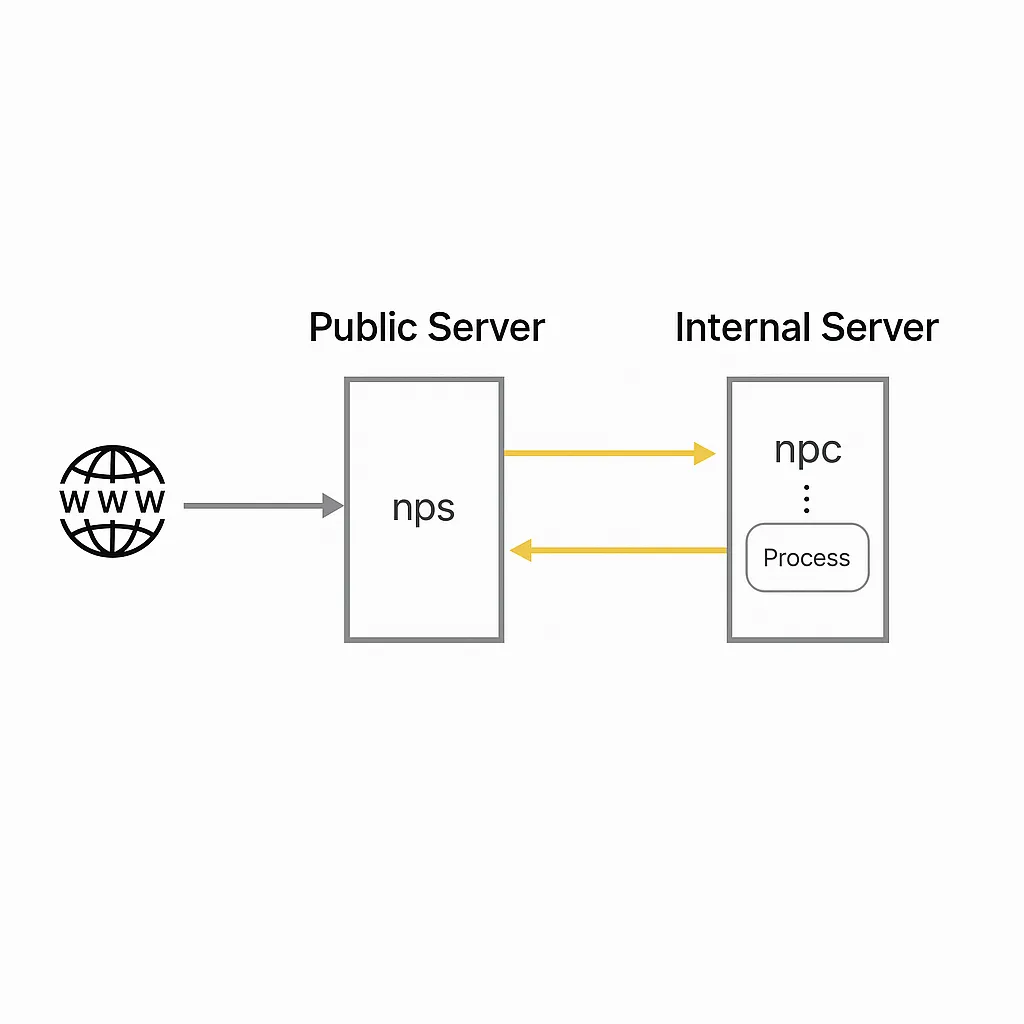
Common NAT Traversal Tools: Principles and Usage
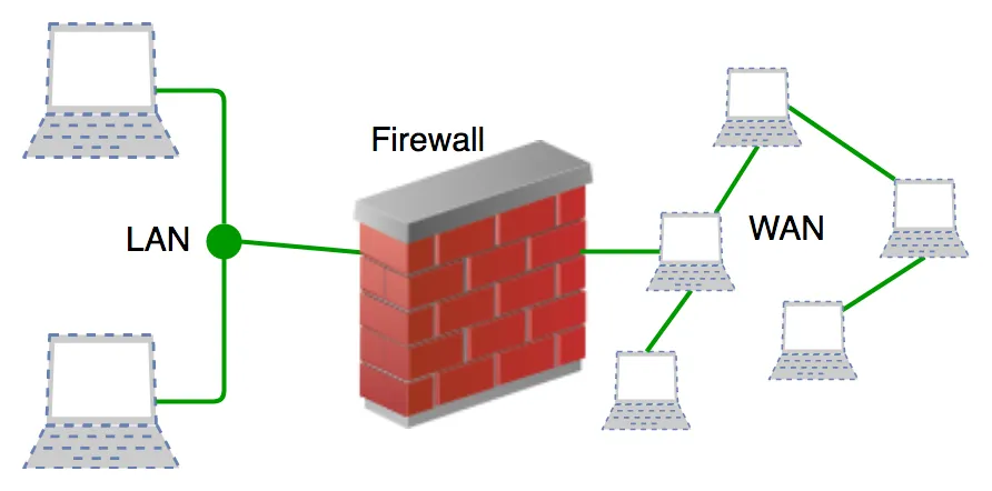
Firewall: Definition and Core Technologies