PCB Manufacturing Defects
PCB manufacturing defects can significantly impact the performance, reliability, and longevity of electronic devices, making it essential for engineers, designers, and manufacturers to understand and address them effectively. This tag, PCB Manufacturing Defects, serves as a comprehensive resource hub for professionals and enthusiasts seeking to identify, prevent, and resolve common issues that arise during the printed circuit board production process. Whether you are troubleshooting a faulty prototype or optimizing a high-volume assembly line, the articles gathered here provide practical guidance on spotting defects early and implementing corrective measures to ensure high-quality outcomes. Common defects include soldering issues like bridging or cold joints, which often stem from improper temperature control or flux application, as well as trace delamination caused by material inconsistencies or environmental stresses. Other prevalent problems encompass via failures, where plating voids lead to connectivity breakdowns, and component misalignment due to stencil inaccuracies. By exploring these topics, you gain actionable insights into root cause analysis techniques, such as using X-ray inspection or automated optical inspection (AOI) tools, which help pinpoint flaws without destructive testing. Best practices highlighted in our content emphasize design for manufacturability (DFM) principles, like incorporating adequate clearances and selecting robust materials, to minimize defects from the outset. For those dealing with real-world challenges, the tag offers case studies and step-by-step tutorials on rework strategies, including safe desoldering methods and conformal coating repairs. Understanding these defects not only reduces scrap rates and production costs but also enhances product safety and compliance with industry standards like IPC-A-610. Dive into the related articles to equip yourself with the knowledge needed to elevate your PCB projects, from hobbyist builds to industrial applications, ensuring fewer failures and more reliable electronics.
Technical Articles
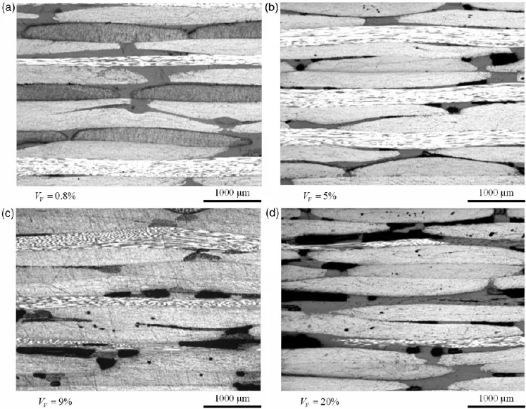
Void Formation in PCB Lamination: Understanding the Mechanisms and Mitigation Strategies
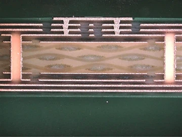
Delamination in PCB Lamination: Causes, Detection, and Prevention
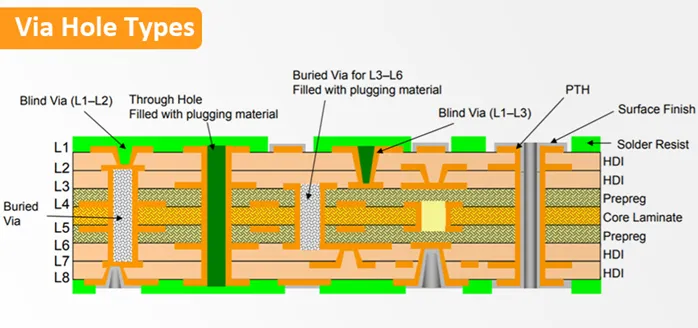
Troubleshooting Challenges in Blind and Buried Via PCB Manufacturing

10 Emerging Cyber Threat Trends and Attack Techniques
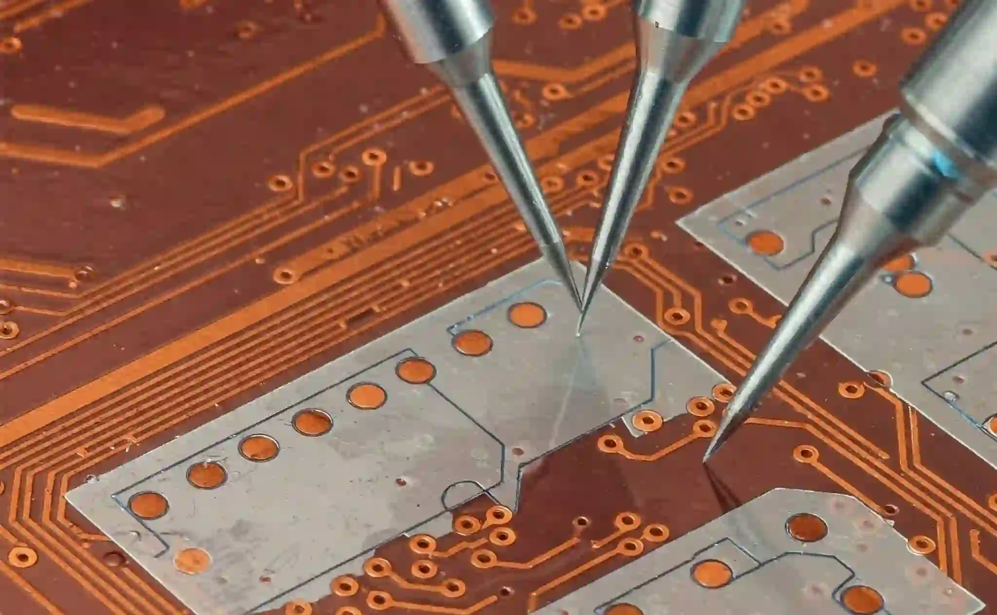
Troubleshooting PCB Etching Problems: Undercutting, Over-Etching, and Uneven Etching
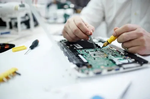
Troubleshooting & Repairing Common PCB Surface Finish Defects
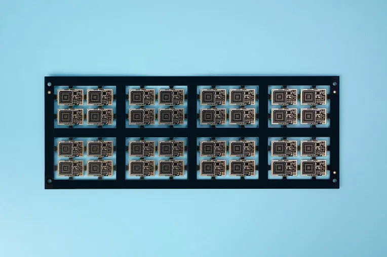
V-Scoring vs. Stamp Hole: Which PCB Depaneling Method is Right for You?

Challenges Faced in PCB Manufacturing
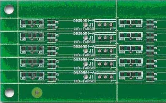
Troubleshooting PCB Panelization: Common Problems and Expert Solutions
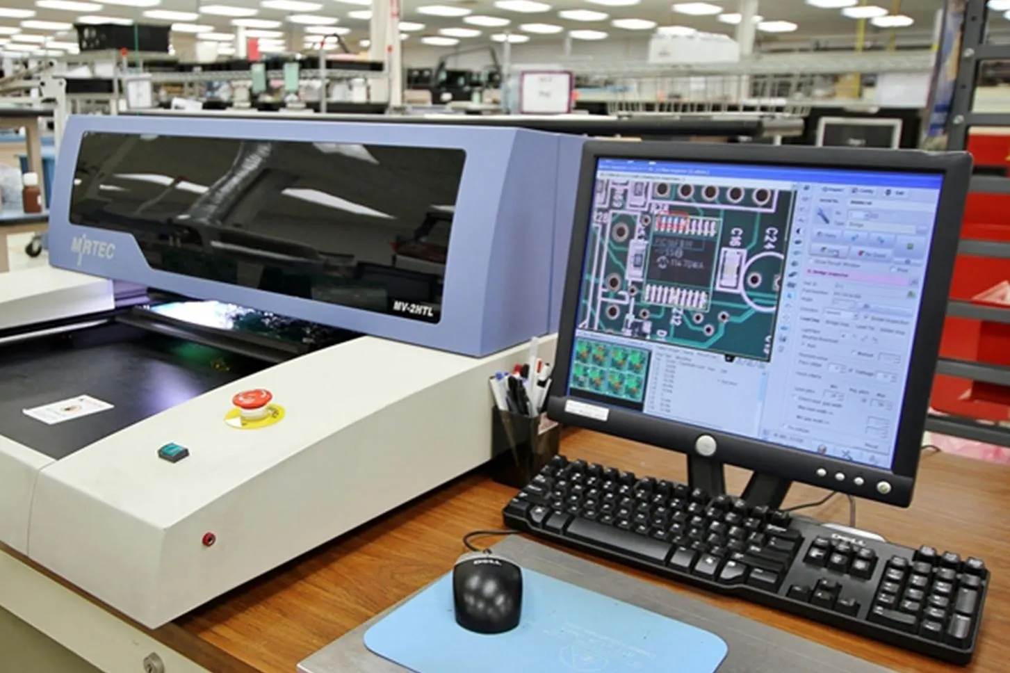
Solder Mask Misalignment: Causes, Consequences, and Solutions for Robust PCB Production

Rogers PCB Manufacturing Defects: Common Issues and How to Avoid Them
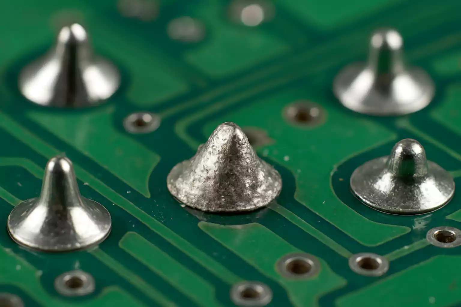
Avoiding the Pitfalls: Common Mistakes in PCB Mass Production and How to Fix Them

Overview of China’s Medical Device Industry

Implementing Automated Conformal Coating for Improved PCB Reliability
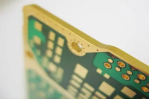
Solving Plated Through-Hole Problems: A PCB Troubleshooting Guide
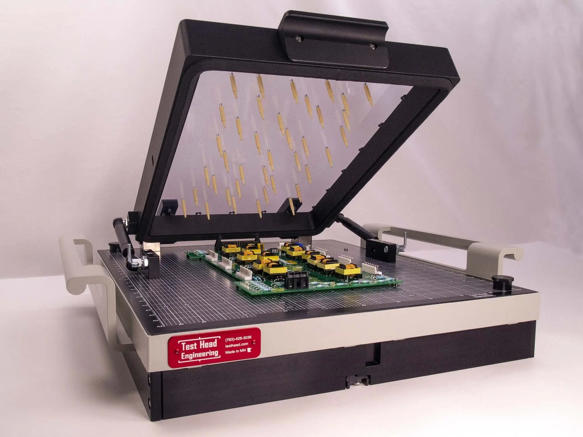
Vacuum vs. Pneumatic ICT Test Fixtures: Which is Right for Your Production Line?
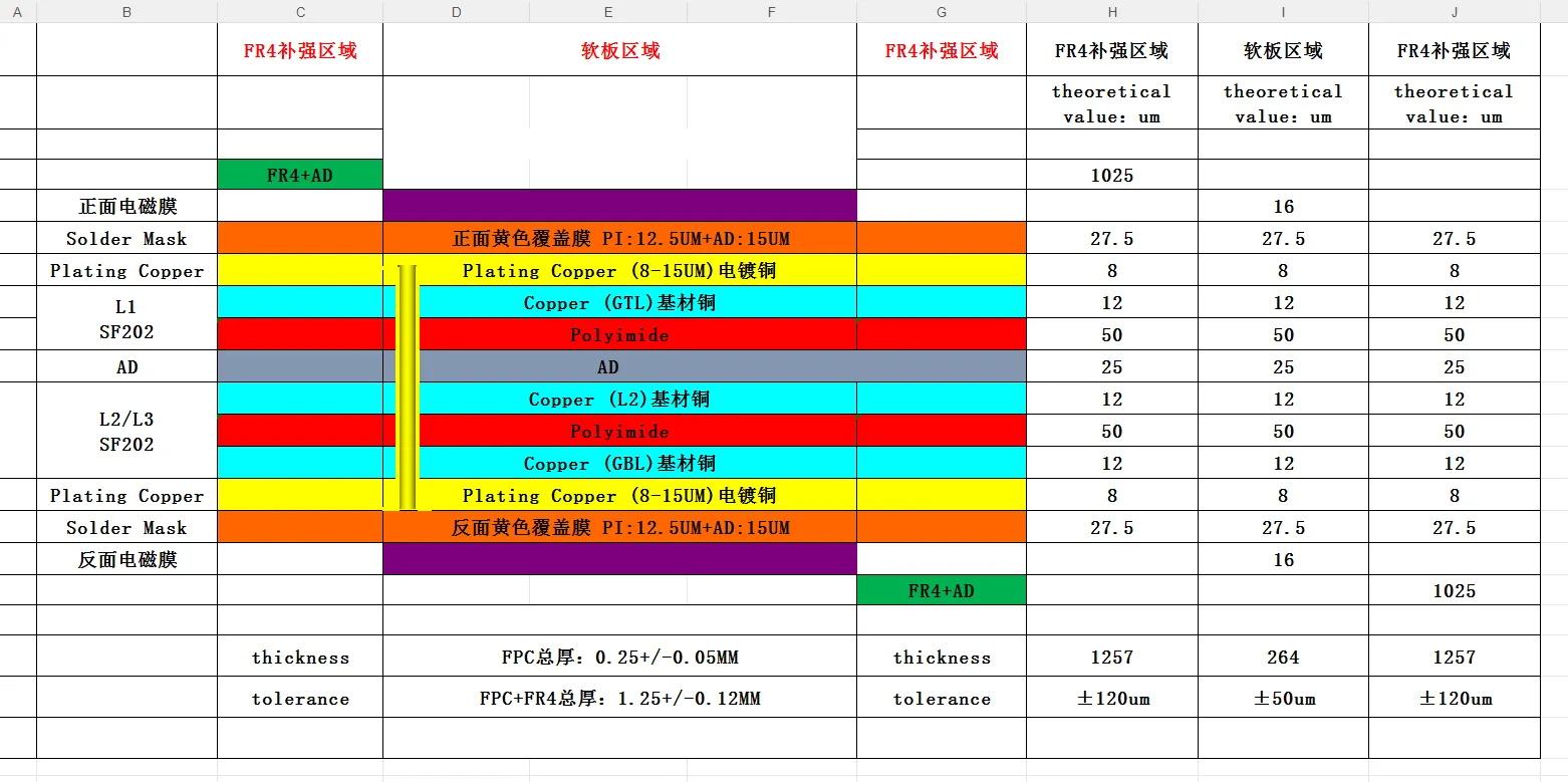
PCB Stackup, Impedance and Thickness Issues in CAM Review
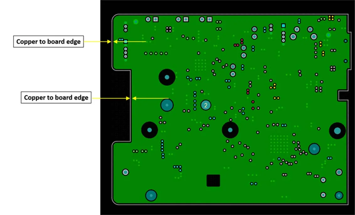
FR4 PCB Edge Clearance: How Much Copper Should Be Kept from the Board Edge?