 00:58
00:58
RF Layout
RF Layout plays a critical role in the design of printed circuit boards (PCBs) that handle radio frequency signals, ensuring optimal performance in high-frequency applications such as wireless communications, radar systems, and IoT devices. This tag encompasses articles and resources focused on the specialized techniques required to manage signal integrity, minimize electromagnetic interference (EMI), and achieve reliable transmission at frequencies ranging from megahertz to gigahertz. For engineers and designers searching for RF Layout guidance, understanding these principles is essential to avoid common pitfalls like signal loss, crosstalk, or unwanted radiation that can compromise device functionality. Key aspects covered under this tag include best practices for trace routing, impedance matching, and ground plane optimization. For instance, proper component placement reduces parasitic capacitance, while controlled impedance lines maintain signal quality over distance. Practical applications extend to designing antennas, amplifiers, and filters where even minor layout errors can lead to significant performance degradation. Readers often seek this information to troubleshoot issues in prototypes or to refine designs for compliance with standards like FCC regulations on emissions. By delving into the content here, you can gain actionable insights into tools like simulation software for predicting RF behavior and real-world case studies that demonstrate successful implementations. Whether you are optimizing a PCB for 5G networks or enhancing RF modules in consumer electronics, the articles tagged with RF Layout provide in-depth explanations and step-by-step approaches to elevate your designs. Exploring these resources can help you apply proven strategies directly to your projects, fostering innovation in high-frequency electronics.
Video Guide
-
00:58
Technical Articles
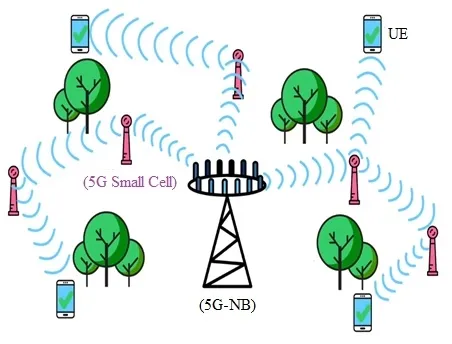
5G Distributed Small Cell Network Structure and Benefits
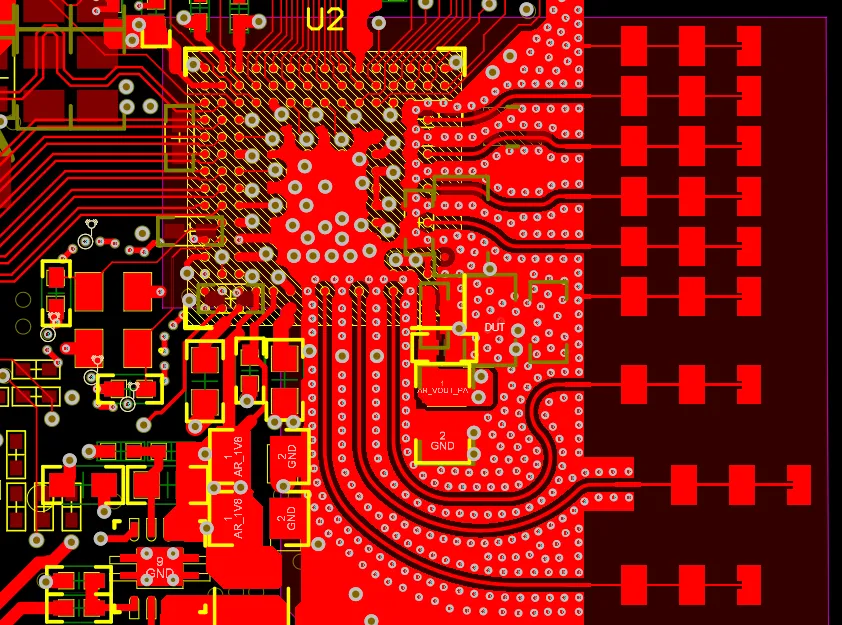
RF PCB Design for Beginners: A Complete Introductory Guide
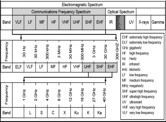
Radio Spectrum Banding for Electromagnetic Warfare
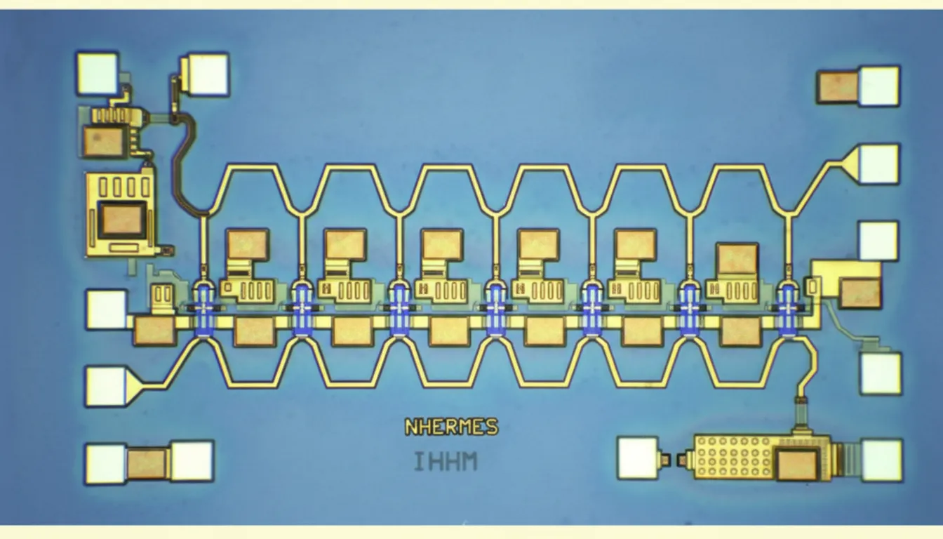
PNA-X Network Analyzer: Key Advantages

Fan Microstrip Structures in RF Amplifiers
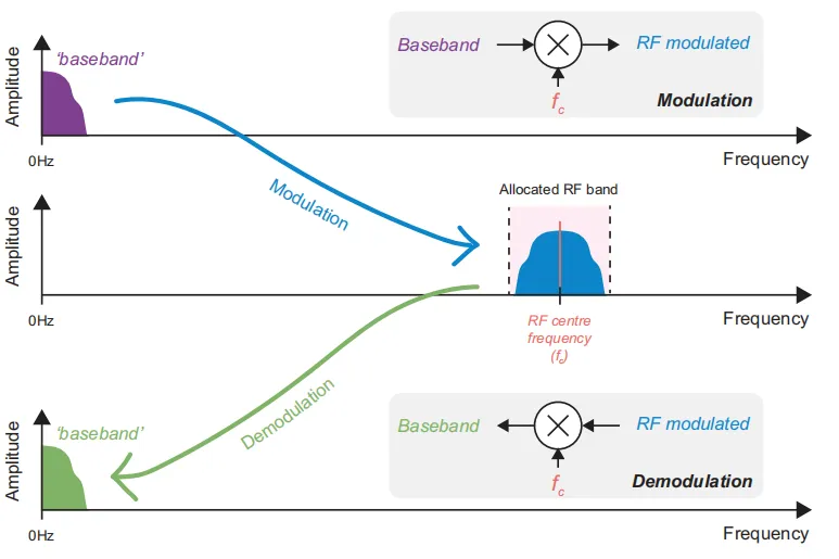
Modulation and Demodulation Methods for Radio Systems
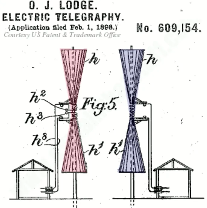
Pioneers of Early Antenna Development
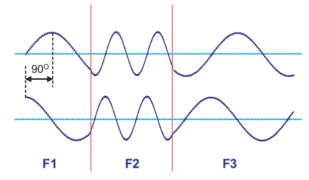
Digital Downconversion and Upconversion Explained

DEVM in FEM RF Amplifier Output Power
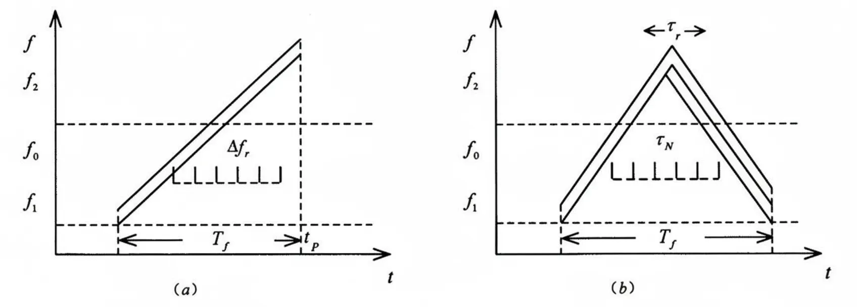
Search Superheterodyne Radar Frequency Measurement
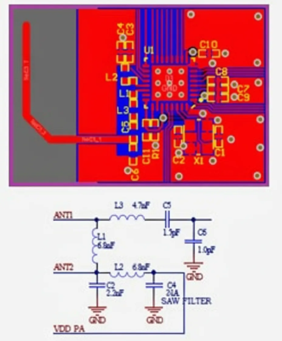
Designing a Smart Wristband with nRF51822

How Do Smartphones Determine Location?

Five Key Points for 5G Testing
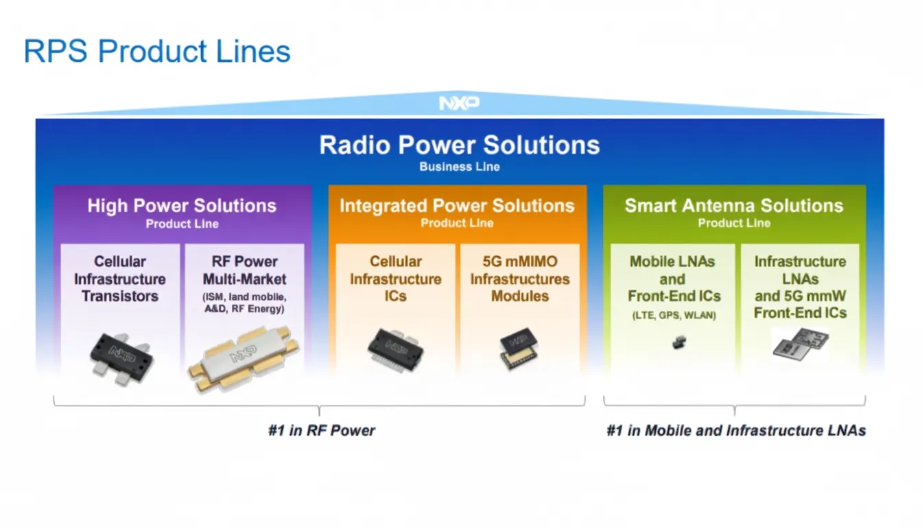
NXP 5G RF Power Device Integration Options
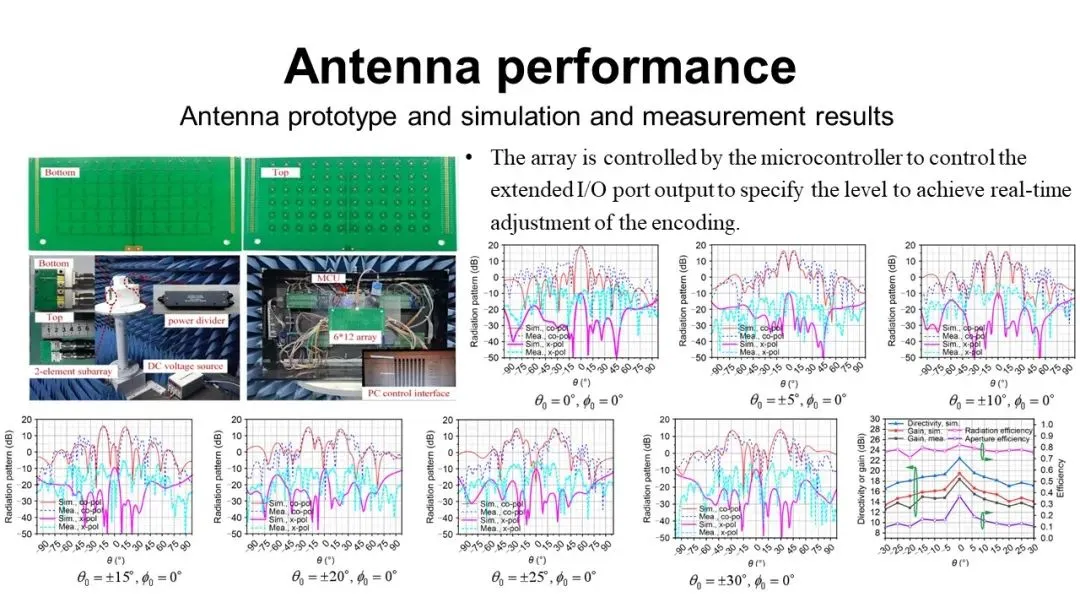
Low-Profile Dual-Polarized Dual-Beam Scanning Antenna Array
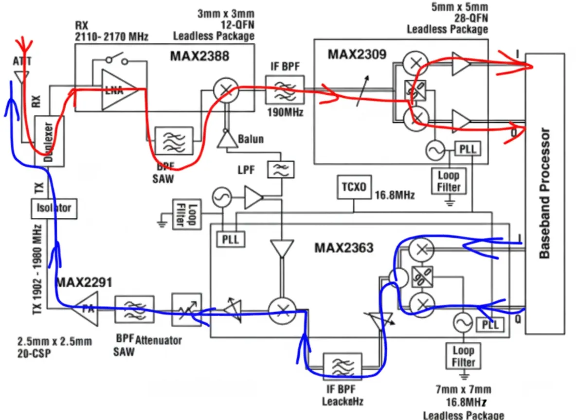
RF Communication System Components and Circuit Diagram
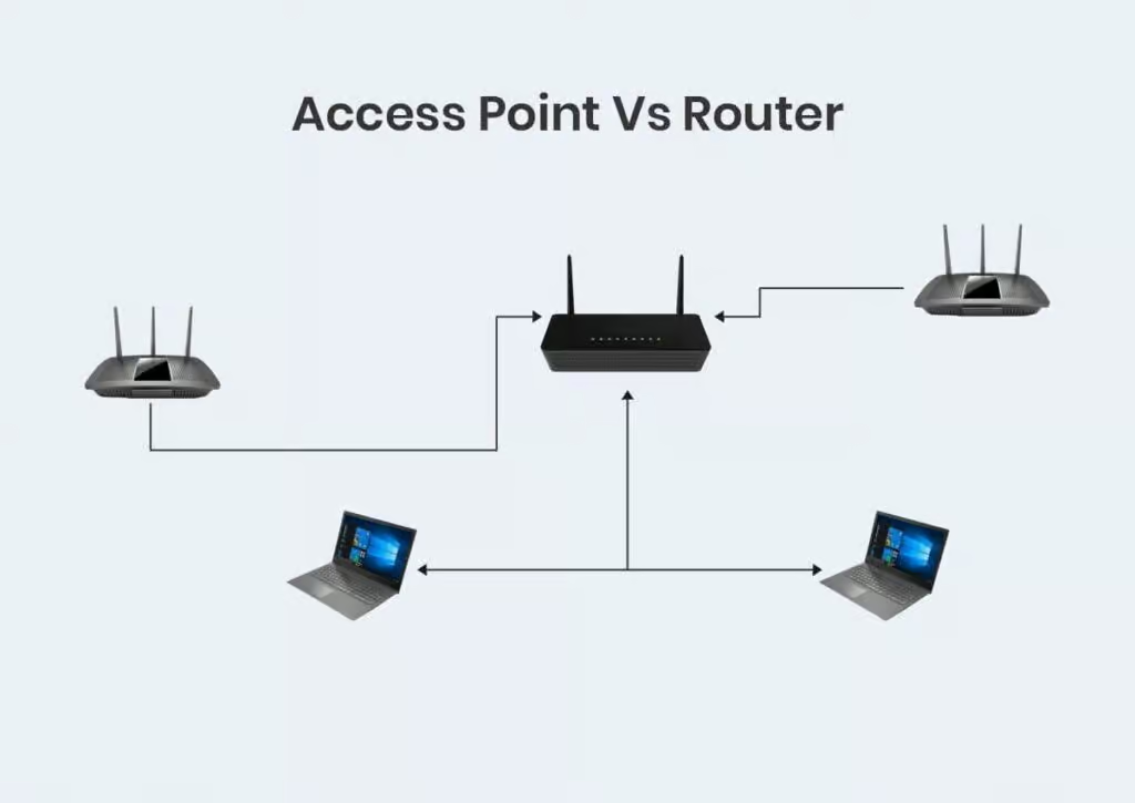
Wireless AP vs Wireless Router: Which Is More Stable
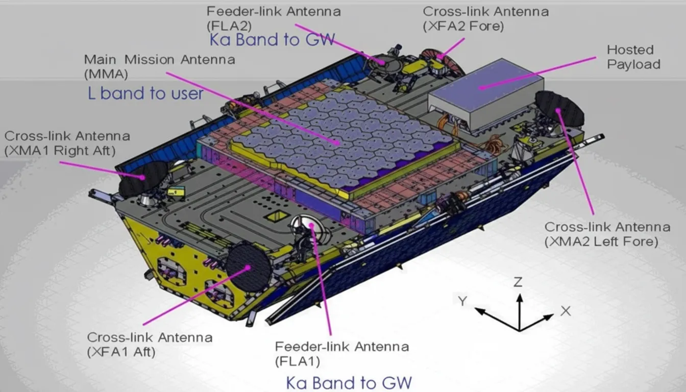
Ka-Band Inter-Satellite Links in the Iridium Constellation
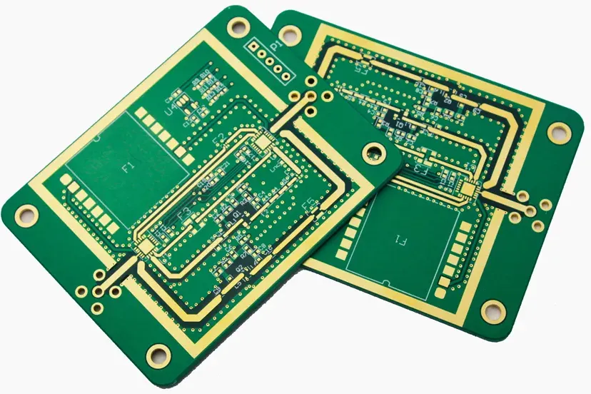
ENIG Surface Finish for High-Frequency PCBs: Impact on Signal Integrity