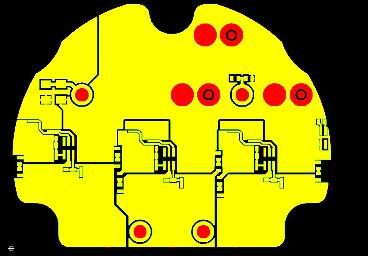
During CAM review of a single-sided aluminum-core PCB measuring 82.12 mm by 207.16 mm, our engineering team identified multiple locations where trace-to-trace and trace-to-copper spacing fell below reliable manufacturing limits. From a DFM perspective, the primary concern was manufacturing stability and the prevention of short circuits after etching and surface finish. Without clarification, the finished boards could have entered production with residual copper bridges that cause electrical shorts, yield loss, and potential assembly failures. This case forms a practical chapter in Aluminum PCB Design Guidelines focused on clearance and process constraints unique to metal-core boards.
The order ( #ALU-20260204-065 ) specified a Guangdong Boyun aluminum substrate with 3.0 W thermal conductivity, 1.6 mm thickness, 1 oz / 3 oz copper, cold-white solder mask on the top side only, black silkscreen, lead-free HASL finish, single-piece shipment with no process edge, 100 % AOI and full high-voltage AC 3000 V testing, and an eight-day delivery window. Quantity was 10 pieces. These parameters are typical for power-moduleor or LED applications that rely on the aluminum base for heat dissipation, yet the combination of tight clearances, oversized holes, and single-sided construction required explicit engineering confirmation before release.
Why This Single-Sided Aluminum Design Triggered Detailed Clearance Checks
Our CAM engineer first measured the minimum distances between adjacent traces and between traces and large copper areas. Several gaps measured below the process capability for 3 oz copper on aluminum-core material. On metal-core PCBs the etching process must completely remove copper from these narrow channels; any residual copper creates a short that may only appear after high-voltage testing or under thermal load.
Additional observations included an 8.6 mm hole that exceeded available drill-bit sizes, solder-mask openings that matched the pad size exactly, silkscreen characters sitting on pads or fused together, and a hole-copper thickness call-out that is irrelevant for a true single-sided board. These secondary items added process complexity, but the insufficient clearance remained the highest-risk issue for electrical integrity.
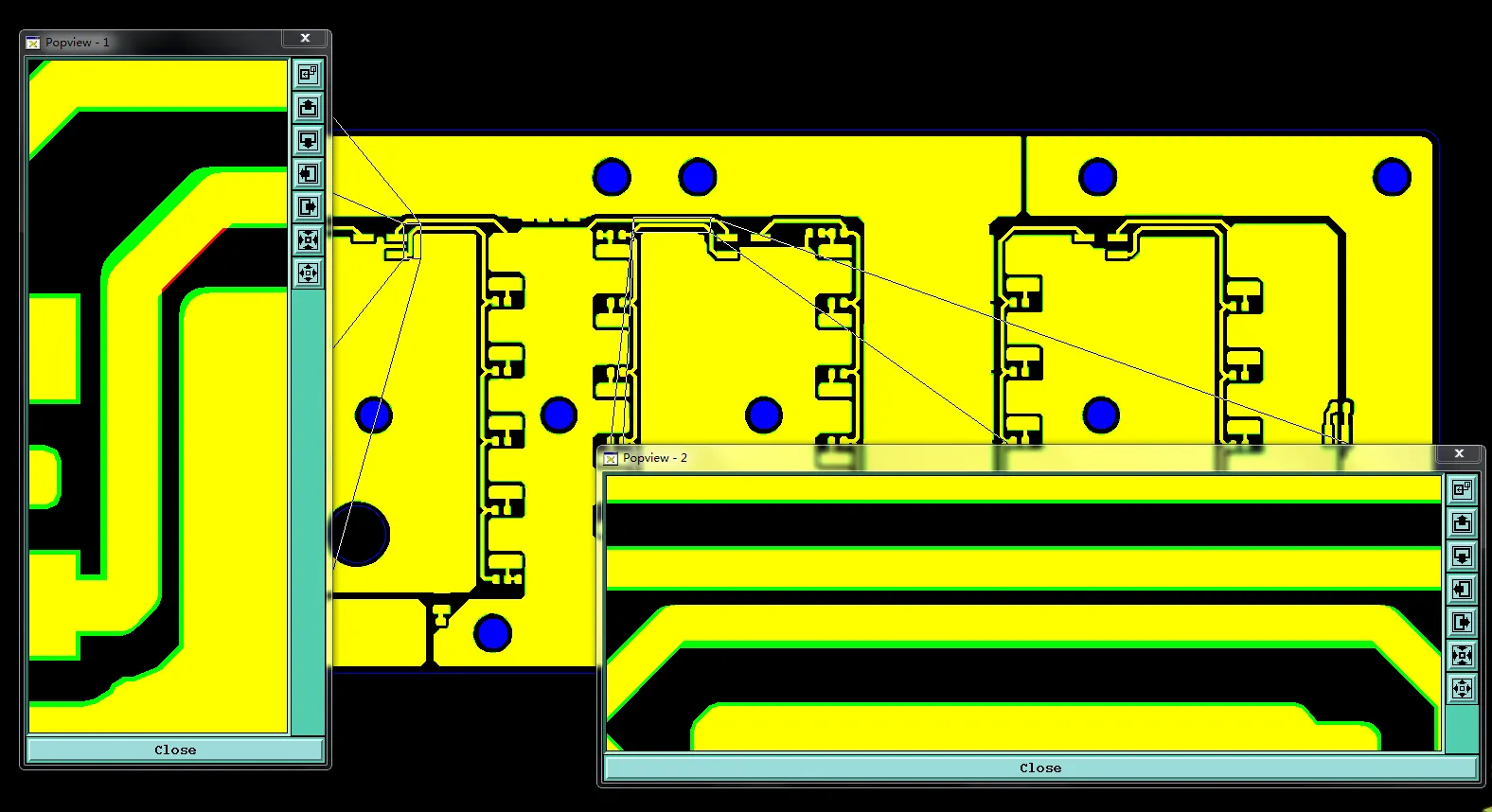
Figure 1: the clearance between traces and between traces and copper areas is too small
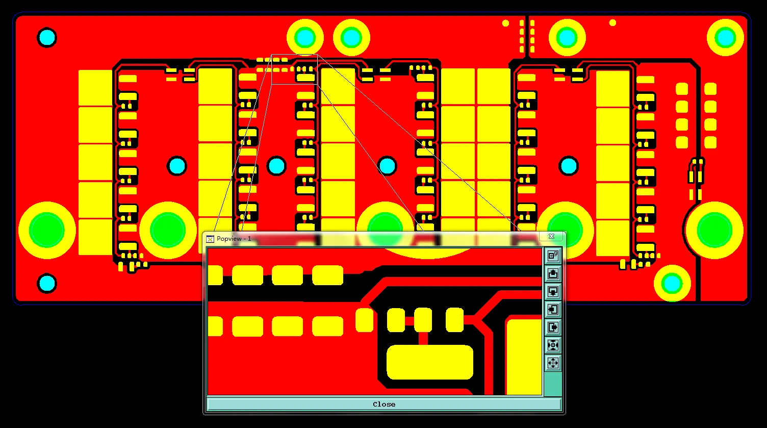
Figure 2: the trace and solder mask pad are the same size
Risk indicators included the 3 oz copper weight (which requires more aggressive etching), the absence of a process edge, the requirement for 100 % high-voltage testing at AC 3000 V, and the single-sided construction that leaves no secondary copper layer to redistribute current if a short forms. On aluminum boards any short also risks localized overheating that can degrade the dielectric layer between copper and aluminum.
| Feature Observed | Condition in Files | Primary DFM Risk |
|---|---|---|
| Trace-to-trace / trace-to-copper spacing | Below process minimum | Short circuits after etching |
| 8.6 mm hole | No matching drill bit | Process change to routing required |
| Solder-mask opening vs pad | Identical size | Potential pad coverage after registration |
Table 1 summarizes the key observations that generated the Engineering Question
Tight Clearance, Large-Hole Processing and Mask Expansion as Core Risks
The dominant risk was insufficient spacing between traces and between traces and copper pours. On a single-sided aluminum board with 3 oz copper the etching undercut is more pronounced; residual copper bridges can remain even when the aluminum PCB design appears compliant on screen. A second risk involved the 8.6 mm hole. No standard drill bit of that diameter was available, so the feature had to be converted to a routed slot with a controlled tolerance of ±0.1 mm. A third risk concerned solder-mask openings that matched the copper pads exactly; any registration shift would allow mask to cover the pad edge and reduce solderable area.
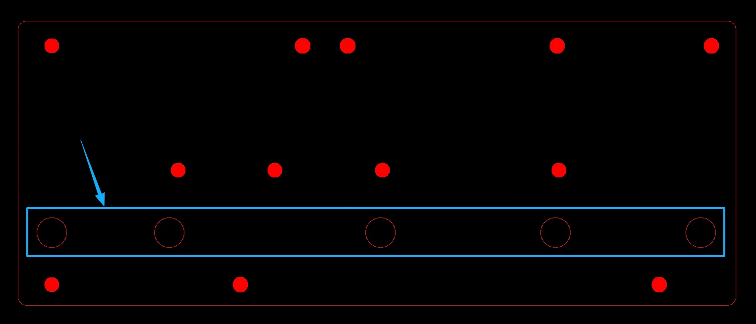
Figure 3: changed the 8.6 mm drilled hole to a routed slot
Secondary observations included silkscreen characters sitting on pads or fused together, and a hole-copper thickness specification that does not apply to a true single-sided construction. These items required confirmation but did not carry the same immediate electrical risk as the clearance and large-hole issues.
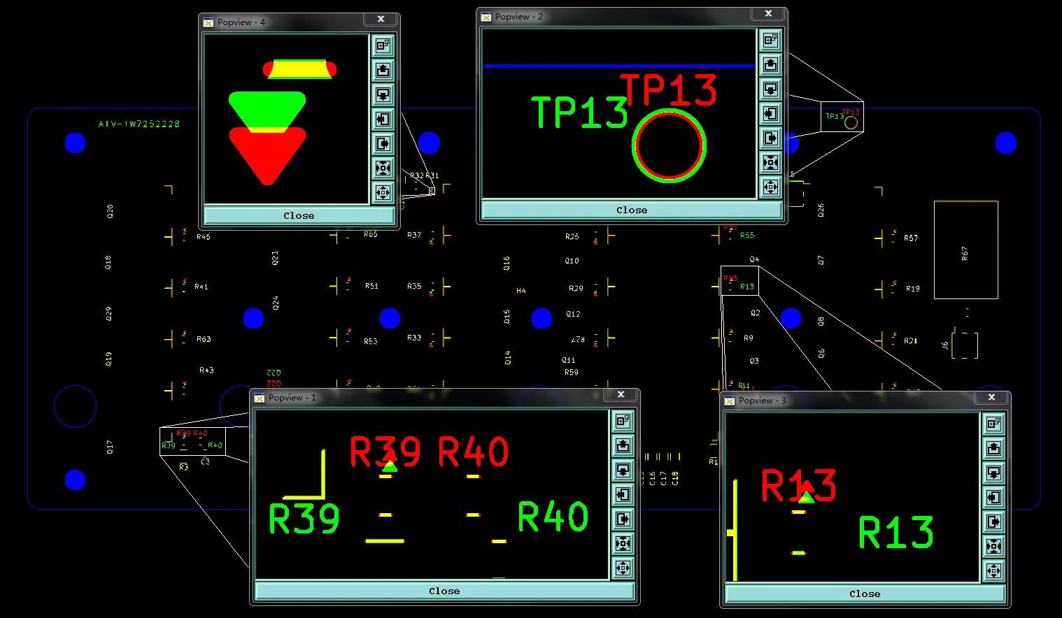
Figure 4: the characters and character frames located on pads or overlapping areas
From a DFM perspective the priority sequence was clear: enlarge critical clearances by moving traces, convert the oversized hole to a routed feature, expand the solder-mask openings by 0.05 mm per side, and document the remaining cosmetic and single-sided adjustments.
How Insufficient Clearance and Process Limits Affect Yield and Reliability
If production had continued without addressing the tight clearances, residual copper bridges would have remained after etching. These bridges create direct short circuits that fail the mandatory 100 % high-voltage AC 3000 V test or, worse, pass initial testing and fail later under thermal load. On an aluminum-core board a short can also produce localized heating that degrades the thin dielectric layer between the copper and the aluminum base, leading to insulation breakdown.
According to common IPC-2221 spacing guidance and IPC-A-600 acceptability criteria, insufficient conductor spacing is classified as a defect that directly impacts electrical performance. On metal-core PCBs the consequence is amplified because heat dissipation relies on the continuous aluminum base; any short-induced hot spot accelerates dielectric aging.
Leaving the 8.6 mm hole as a drilled feature was impossible without the correct bit. Attempting to force a smaller drill would have produced an undersized hole and potential breakout. Converting it to a routed slot with ±0.1 mm tolerance restores dimensional control while remaining within mechanical capability.
Identical solder-mask and pad sizes leave no margin for registration tolerance. Even a small shift can allow mask to encroach on the pad, reducing the solderable area and creating weak joints during HASL or subsequent assembly. Silkscreen characters on pads or fused together produce similar cosmetic and functional interference.
| Potential Failure Mode | Root Cause Linked to EQ | Production or Field Impact |
|---|---|---|
| Electrical short circuits | Trace spacing below process limit | High-voltage test failure, scrap |
| Undersized or irregular hole | 8.6 mm feature without matching drill | Mechanical fit failure, yield loss |
| Reduced solderable pad area | Solder-mask opening equal to pad | Weak joints, assembly rejects |
| Silkscreen interference | Characters on pads or fused | Cosmetic rejects, solder defects |
Table 2 maps each realistic failure mode to the Engineering Question items.
What Happens When Tight Clearances and 8.6 mm Holes Remain Uncorrected on Metal-Core PCBs
Had the original tight clearances remained, boards would have failed the mandatory high-voltage AC 3000 V test or, worse, passed initial screening and developed intermittent shorts after thermal cycling. Localized heating at a residual copper bridge could also degrade the dielectric layer, producing insulation failures that appear only after the product is in service.
Leaving the 8.6 mm feature as a drilled hole was not feasible. An incorrect bit would have produced an undersized or irregular opening that fails mechanical fit or creates stress concentrations in the aluminum base. Converting it to a routed slot with controlled tolerance eliminates that risk.
Identical solder-mask and pad geometries would have allowed mask encroachment after normal registration variation, reducing the effective solderable area under lead-free HASL. Silkscreen characters remaining on pads or fused together would have created additional surface defects that interfere with soldering or visual acceptance. All of these scenarios share a common origin: insufficient design-for-manufacturing margin on a metal-core board.
Preventive Actions Confirmed During the DFM Exchange
Our engineering team issued a focused Engineering Question that first addressed the insufficient clearances. Traces were carefully moved to restore safe spacing while preserving electrical connectivity. This adjustment eliminates residual copper bridges and protects the high-voltage test yield.
For the 8.6 mm hole the team proposed converting the feature to a routed slot with a tolerance of ±0.1 mm. The customer accepted the change, restoring dimensional accuracy without requiring non-standard tooling. Solder-mask openings were enlarged by 0.05 mm per side to provide registration margin and prevent pad coverage. Silkscreen characters located on pads or fused together were enlarged, moved, or accepted as partially incomplete where necessary. Because the board is truly single-sided, the hole-copper thickness requirement was documented as not applicable.
Production numbering was added to the character layer as requested. With all decisions confirmed, the CAM files were updated and the order released under the eight-day schedule. The revised design retained the intended thermal and electrical performance while eliminating the primary sources of short circuits, dimensional error, and surface defects.
| Action Item | Customer Decision | Manufacturing Benefit |
|---|---|---|
| Trace clearance | Traces moved to restore spacing | No residual copper bridges, high-voltage test pass |
| 8.6 mm hole | Converted to routed slot ±0.1 mm | Dimensional accuracy without special tooling |
| Solder-mask opening | Enlarged 0.05 mm per side | Full pad exposure after registration |
Table 3 records the closed-loop decisions that converted a high-risk aluminum design into a manufacturable product.
Why Early Clearance Verification Remains the Highest-Leverage Step in Aluminum PCB
This case demonstrates that tight trace clearances and oversized features on single-sided aluminum PCBs are not minor layout details; they constitute direct threats to electrical safety, high-voltage test yield, and mechanical fit. By identifying the insufficient spacing, converting the large hole to a controlled routed slot, and expanding the solder-mask openings during CAM review, the engineering team protected both first-pass yield and long-term reliability.
Designers working with metal-core boards are encouraged to maintain adequate trace-to-trace and trace-to-copper clearances for the chosen copper weight, verify that all hole sizes fall within available tooling, provide solder-mask expansion margins, and request early DFM feedback on single-sided construction details. These practices convert potential manufacturing problems into controlled, documented decisions before production begins.
Proactive clearance and process verification remain among the highest-leverage actions a DFM team can take when releasing aluminum-core PCBs for power or LED applications.
FAQ
Q: Why is trace clearance more critical on aluminum PCBs with 3 oz copper?
A: Heavier copper requires longer etching time and produces greater undercut. Narrow gaps can retain residual copper bridges that create shorts, especially under the mandatory high-voltage test required for many metal-core designs.
Q: What happens if an oversized hole cannot be drilled on an aluminum board?
A: Forcing an incorrect bit produces an undersized or irregular opening that fails mechanical fit. Converting the feature to a routed slot with a controlled tolerance restores dimensional accuracy without special tooling.
Q: Why expand solder-mask openings by 0.05 mm per side on aluminum PCBs?
A: Registration tolerance can shift the mask relative to the copper. Identical mask and pad sizes leave no margin; a small expansion ensures the entire pad remains exposed for reliable HASL and soldering.
Q: Can residual copper bridges pass initial testing yet fail later?
A: Yes. Thin residual bridges may survive low-voltage continuity checks but fail under high-voltage stress or thermal cycling, producing intermittent shorts or dielectric breakdown between copper and the aluminum base.
Q: Why ignore hole-copper thickness on a single-sided aluminum board?
A: True single-sided constructions have no plated through-holes that require copper thickness control. Specifying a hole-copper value creates an unnecessary process constraint that can be safely omitted after confirmation.
Q: How can designers avoid similar issues on future aluminum PCBs?
A: Maintain clearances appropriate for the copper weight, verify that all hole diameters fall within available tooling, provide solder-mask expansion margins, keep silkscreen clear of pads, and request early DFM review. These steps form the core of reliable Aluminum PCB Design Guidelines.
```