In a BUCK converter, fast turn-on and turn-off of the MOSFET is the key to cutting switching loss. That requirement depends on the front-end gate drive working together with a hysteretic comparator. The following covers the circuit structure and the parameter calculations for the hysteretic block.
Why Use a Push-Pull Stage to Drive the MOSFET?
Fast switching needs a strong front-end drive. A bipolar push-pull stage is a common solution. With the drive rail set to 12 V, the core behavior is as follows.
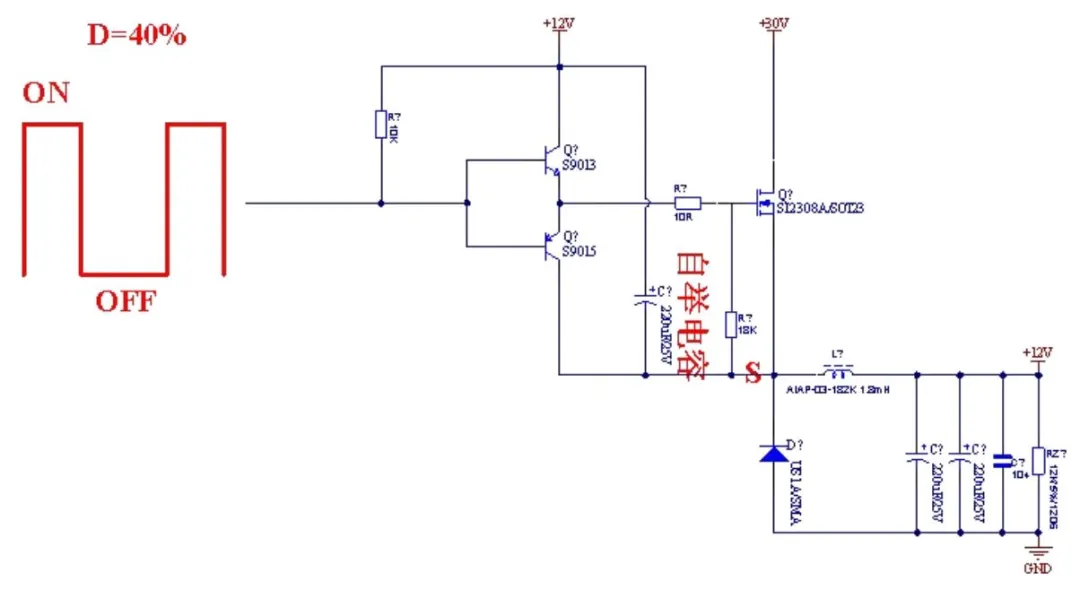
Figure 1 | BUCK topology and push-pull drive
When the circuit is in the ON state:
The NPN transistor (S9013) conducts, with base current Ib of about 1 mA. The 12 V rail charges the MOSFET CGS through a 10 Ω resistor. When VGS reaches 3 V, the MOSFET starts to conduct and current flows into the following power stage.
When the circuit is in the OFF state, CGS discharges through two paths: through the 10 Ω resistor into the PNP transistor (S9015), and through the pull-down resistor. When VGS falls below 3 V, the MOSFET turns fully off and extra loss is avoided.
The advantage of the push-pull stage is fast charge in ON and fast discharge in OFF, which matches the need for fast MOSFET switching.
How to Build the Hysteretic Comparator, and Why Use Positive Feedback?
Stable BUCK operation also needs a hysteretic comparator. It produces a triangle wave. A second comparator then turns that waveform into PWM that switches the MOSFET. The first task is the hysteretic comparator itself.
1. Device Choice: Why LM393DT?
The supply is 12 V, so the comparator must accept a wide input range. On cost and availability, LM393DT (SO-8) is used. It fits a 12 V system, and the dual-comparator package covers both the triangle-wave generator and the PWM comparator.
2. Circuit Construction: Positive Feedback Is the Key
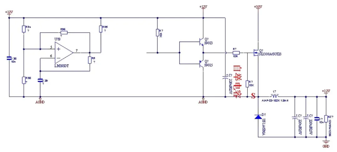
Figure 2 | BUCK circuit with hysteretic comparator
Two points in the hysteretic comparator are easy to mix up:
- Non-inverting input: connect a resistor divider (for example R94 and R98) and a series positive-feedback resistor. Positive feedback is not used here to stabilize the loop (that is the role of negative feedback). It steepens the comparator rising and falling edges so the large "corner" during capacitor charge and discharge—an abrupt, poorly shaped voltage step—is avoided and the triangle wave is cleaner.
- Inverting input: connect the capacitor directly. Charge and discharge of that capacitor produce the voltage change that trips the comparator. That is how the triangle wave is generated.
- Charge/discharge path: a resistor (for example R5) from the comparator output to one end of the capacitor sets the charge and discharge rate.
Parameter Calculation: Thresholds, Resistors, and Capacitance
After the topology is fixed, the component values are calculated. The goals are to keep the capacitor away from the large charge/discharge corner and to meet the frequency target (20 kHz in this example).
1. Set the Thresholds: 8 V High, 4 V Low
To avoid an abrupt voltage step on the capacitor, take one-third of the 12 V rail as the low threshold (4 V) and two-thirds as the high threshold (8 V):
- When the capacitor voltage charges to 8 V, the comparator output goes low and the capacitor starts to discharge.
- When the capacitor voltage discharges to 4 V, the comparator output goes high and the capacitor charges again. The cycle produces a smooth triangle wave between 4 V and 8 V.
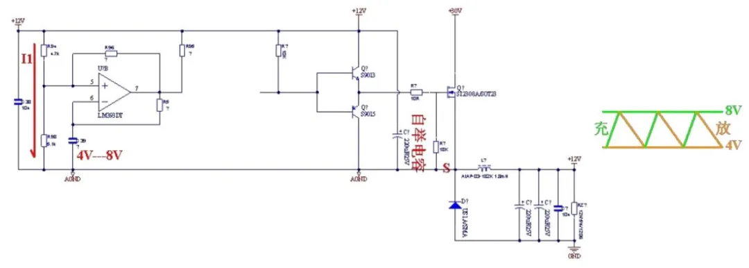
Figure 3 | Hysteretic comparator threshold voltages
2. Calculate the Resistors: Fix the Divider Current, Then Split the Divider
Set the divider loop current (I1) to 1 mA as a balance of power and stability. With a 12 V rail, R94 + R98 would be about 12 V / 1 mA = 12 kΩ. In practice the total is taken near 10 kΩ after debug, which gives:
- R94 = 4.7 kΩ (a common, easy-to-buy value)
- R98 = 5.1 kΩ (4.7 kΩ + 5.1 kΩ ≈ 10 kΩ, close to the calculated total)
The remaining resistors (R95 and R96) are calculated in two states.
Case 1: Comparator output high — calculate R95
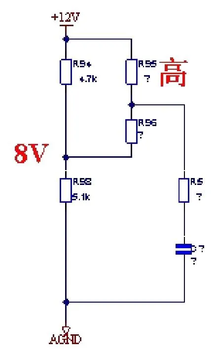
Figure 4 | Equivalent loop with output high
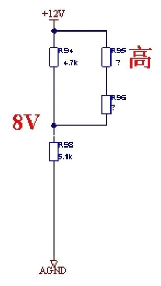
Figure 5 | Equivalent circuit with the charge path removed
The capacitor charge path must not pull the divider voltage. Charge/discharge resistor R5 must therefore be much larger than the divider resistors (R95, R96) so it does not clamp the divider node. R5 is taken as 20 kΩ, well above the 10 kΩ divider total. Checking with the internal-resistance method confirms that R5 does not disturb the divider. The result is R95 ≈ 1.216 kΩ.
Case 2: Comparator output low — calculate R96
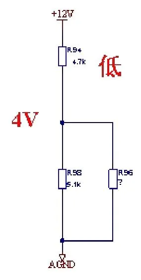
Figure 6 | Equivalent loop with output low
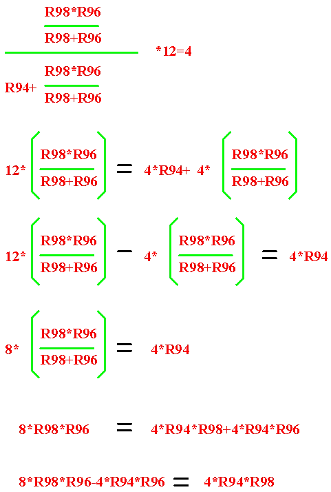
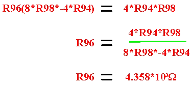
Figure 7 | Derivation of R96
With the low threshold at 4 V, write the superposition equations and substitute R94 = 4.7 kΩ and R98 = 5.1 kΩ. The result is R96 ≈ 4.358 kΩ.
3. Calculate the Capacitor at 20 kHz
The last step is capacitor C at target frequency f = 20 kHz. The derivation uses the capacitor charge equation I dt = C ΔV, where ΔV is the voltage span 8 V − 4 V = 4 V.
The maximum charge current on the capacitor is:

The minimum charge current is zero. The average charge current is:

The maximum discharge current is:

The minimum discharge current is:

The average discharge current is then:

The voltage span on the capacitor is written as ΔV:

The capacitor current-charge relation is:
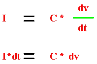
For charging:

For discharging:

Taken together:

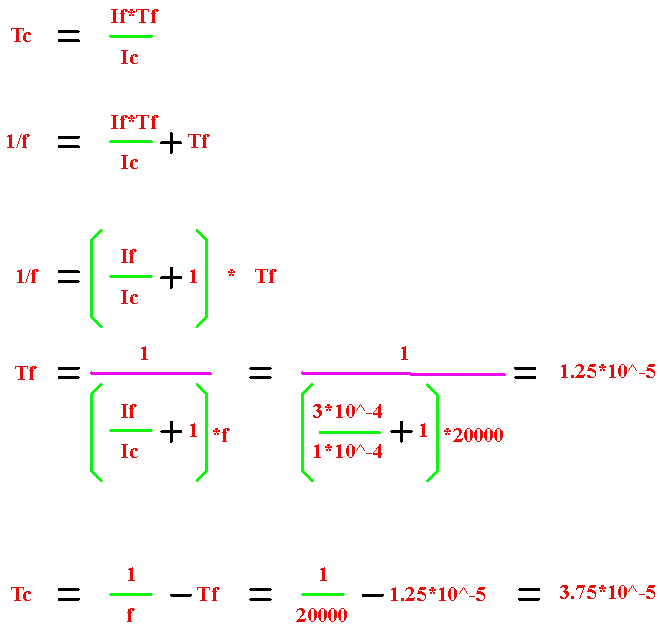
With triangle-wave frequency f = 20 kHz:

Because Ic × Tc = If × Tf:
Using the charge and discharge equations separately for C:
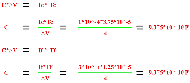
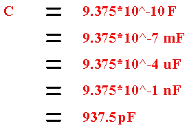
The resulting capacitance is C = 9.375 × 10⁻¹⁰ F.
Key calculation steps
- Maximum charge current Icmax = (8 V − 4 V) / 20 kΩ = 2 × 10⁻⁴ A
- Average charge current Ic = Icmax / 2 = 1 × 10⁻⁴ A
- Maximum discharge current If1 = 8 V / 20 kΩ = 4 × 10⁻⁴ A
- Minimum discharge current If2 = 4 V / 20 kΩ = 2 × 10⁻⁴ A
- Average discharge current If = (If1 + If2) / 2 = 3 × 10⁻⁴ A
Using equal charge and discharge (Ic × Tc = If × Tf, where Tc is charge time and Tf is discharge time) and f = 1 / (Tc + Tf) = 20 kHz gives C ≈ 937.5 pF.
Practical selection: 1 nF (102, X7R)
937.5 pF is not a standard catalog value, so the nearest value 1 nF is used (102 marking, X7R dielectric). During bring-up, measure the triangle-wave frequency with an oscilloscope and trim the capacitor if needed.
Summary
- Circuit structure: the push-pull driver provides fast MOSFET switching; the hysteretic comparator produces a stable triangle wave. Together they form the core of this BUCK control path.
- Parameter logic: set the thresholds at 4 V–8 V to stay off the large waveform corner; fix the divider current first, then split the divider resistors; calculate C from frequency and pick a standard value.
- Lab work: the calculation is the starting point. Measure frequency and voltage on an oscilloscope and trim the resistors and capacitor until the circuit runs stably.