










PCB Knowledge
Printed circuit boards (PCBs) form the backbone of modern electronics, enabling everything from smartphones to industrial machinery. In our PCB Knowledge category, we delve into the essential principles, techniques, and innovations that drive this field forward. Whether you are an engineer refining your designs or a hobbyist embarking on your first project, this collection offers valuable resources to enhance your understanding and skills. The scope of PCB Knowledge spans foundational concepts such as circuit layout and component selection, extending to advanced topics like high-speed signal integrity and thermal management. We provide detailed guides that walk through design software usage, manufacturing processes, and quality assurance methods. Tutorials offer hands-on instructions for prototyping and assembly, while insights from industry experts share real-world case studies and emerging trends. Best practices emphasize reliability, cost efficiency, and compliance with standards like IPC, ensuring your projects meet professional benchmarks. The practical value lies in its direct applicability to everyday challenges. For instance, articles on troubleshooting common PCB failures can save time and resources in product development cycles. Discussions on materials science reveal how choices in substrates and coatings impact performance in harsh environments, such as automotive or aerospace applications. By addressing these elements, PCB Knowledge equips you with tools to innovate and optimize electronic systems that power renewable energy solutions, medical devices, and consumer gadgets. As you read through the articles here, you will gain a comprehensive perspective that connects theoretical knowledge with tangible outcomes. This category serves as a hub for ongoing learning, where each piece builds on the others to foster expertise in PCB technology. Stay informed on the latest advancements, from flexible PCBs to sustainable manufacturing, and apply these insights to your work for superior results.
Latest Blogs
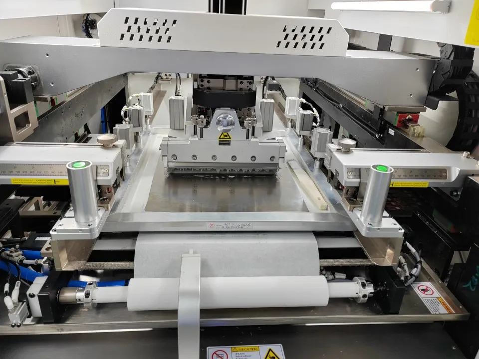
Mobile Phone PCB Assembly Process: SMT and Reflow Soldering Explained
Grasp the SMT assembly process for mobile phone PCBs with focus on reflow soldering PCB, solder paste application, component placement accuracy, and wave soldering. Practical steps, best practices, and troubleshooting help electric engineers achieve reliable high-volume production and minimize defects.
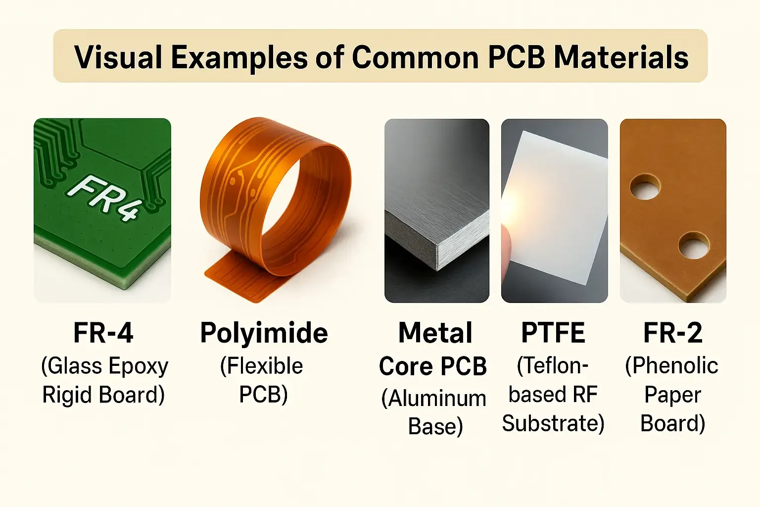
Mobile Phone PCB Materials Guide: Choosing the Right Substrate
Selecting the right substrate matters for mobile phone PCBs. This guide covers FR4 PCB, polyimide PCB, high frequency laminates and material selection criteria like dielectric constant for signal integrity, thermal stability and mechanical reliability. Practical insights help electrical engineers build durable smartphone boards.
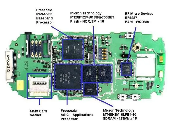
Component Placement Strategies for Optimal Mobile Phone PCB Performance
Strategic SMT component placement enhances mobile phone PCB performance by minimizing signal path, optimizing thermal layouts, and improving power distribution. Follow PCB routing guidelines and best practices for signal integrity, heat dissipation, and reliable high-density designs used by engineers.
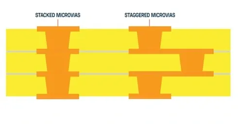
Stacked Vias vs. Staggered Vias: Choosing the Right Via for Your PCB Project
This stacked vs staggered via comparison covers advantages of stacked vias for density and signals against staggered vias for reliability and cost. Practical insights help electric engineers pick the best via type for HDI PCB projects and ensure design success.
Through Hole Via Placement Strategies for Optimal Signal Routing
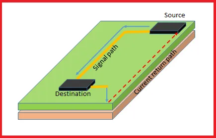
Through hole via placement strategies enhance PCB routing and signal integrity for high speed designs. Via stitching ensures plane continuity, ground vias support return paths, and optimal positioning minimizes crosstalk and EMI. Practical tips help engineers achieve reliable performance in complex boards.
Cost Effective Through Hole Via Design: Balancing Performance and Budget
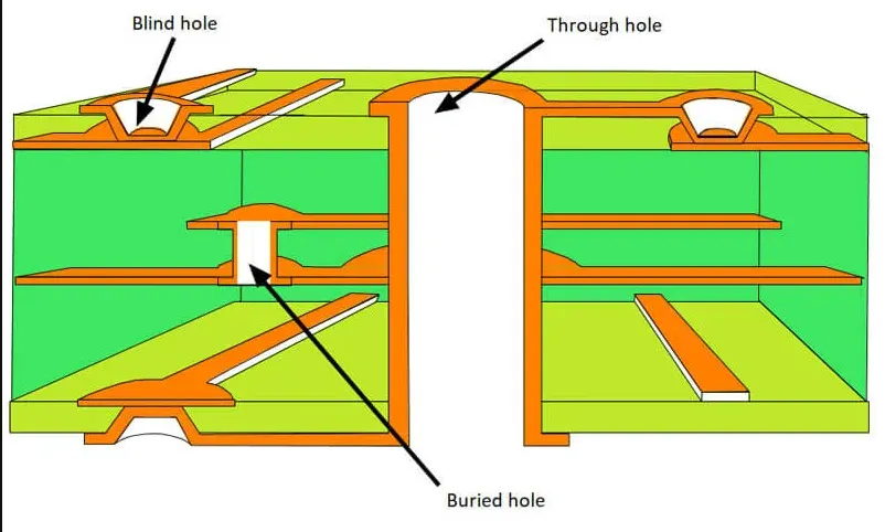
Cut through hole via cost in PCB manufacturing with practical design optimization strategies. Cover drill sizes, aspect ratios, via alternatives, and best practices to balance budget and reliability for electric engineers seeking to minimize PCB costs effectively.
Through Hole Via Reliability: Common Failure Modes and Prevention
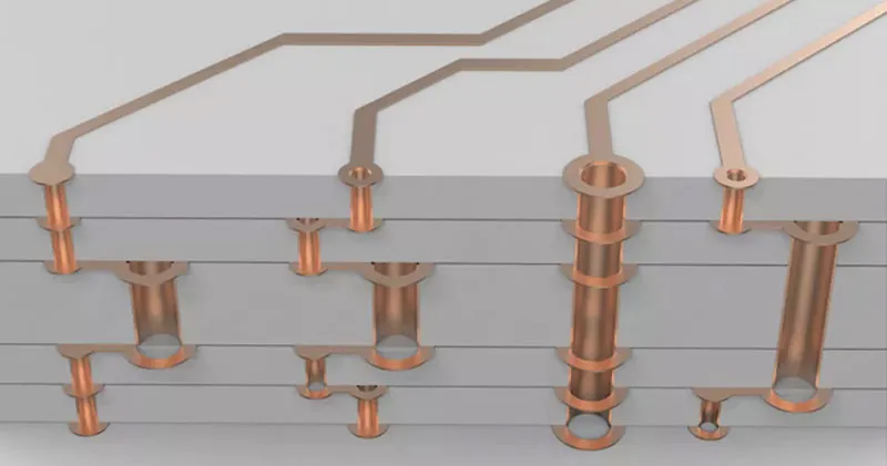
Discover through-hole via reliability challenges including cracking, electromigration, and thermal stress failures in multilayer PCBs. Learn proven prevention strategies, PCB failure analysis techniques, and best practices to boost board longevity in aerospace, automotive, and high-reliability applications.
1 oz Copper PCBs for IoT Devices: Design Considerations and Best Practices
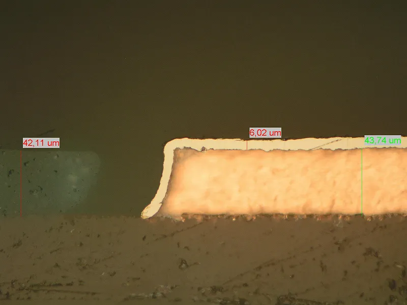
1 oz copper PCBs fit IoT devices perfectly for low-power and wireless needs. This guide covers IoT PCB design 1 oz copper, trace routing, signal integrity, antenna design 1 oz copper, small PCB design tips, and best practices to ensure reliability and efficiency for electrical engineers.
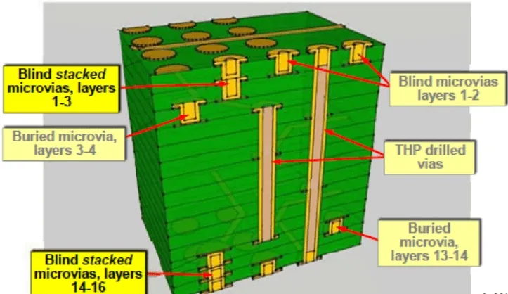
Troubleshooting Stacked Via Problems: A Practical Guide
Step-by-step troubleshooting for stacked via failure analysis tackles cracks, delamination, and open circuits in HDI PCBs. Covers causes, inspection methods, best practices, and IPC standards to boost reliability and cut production issues for engineers.
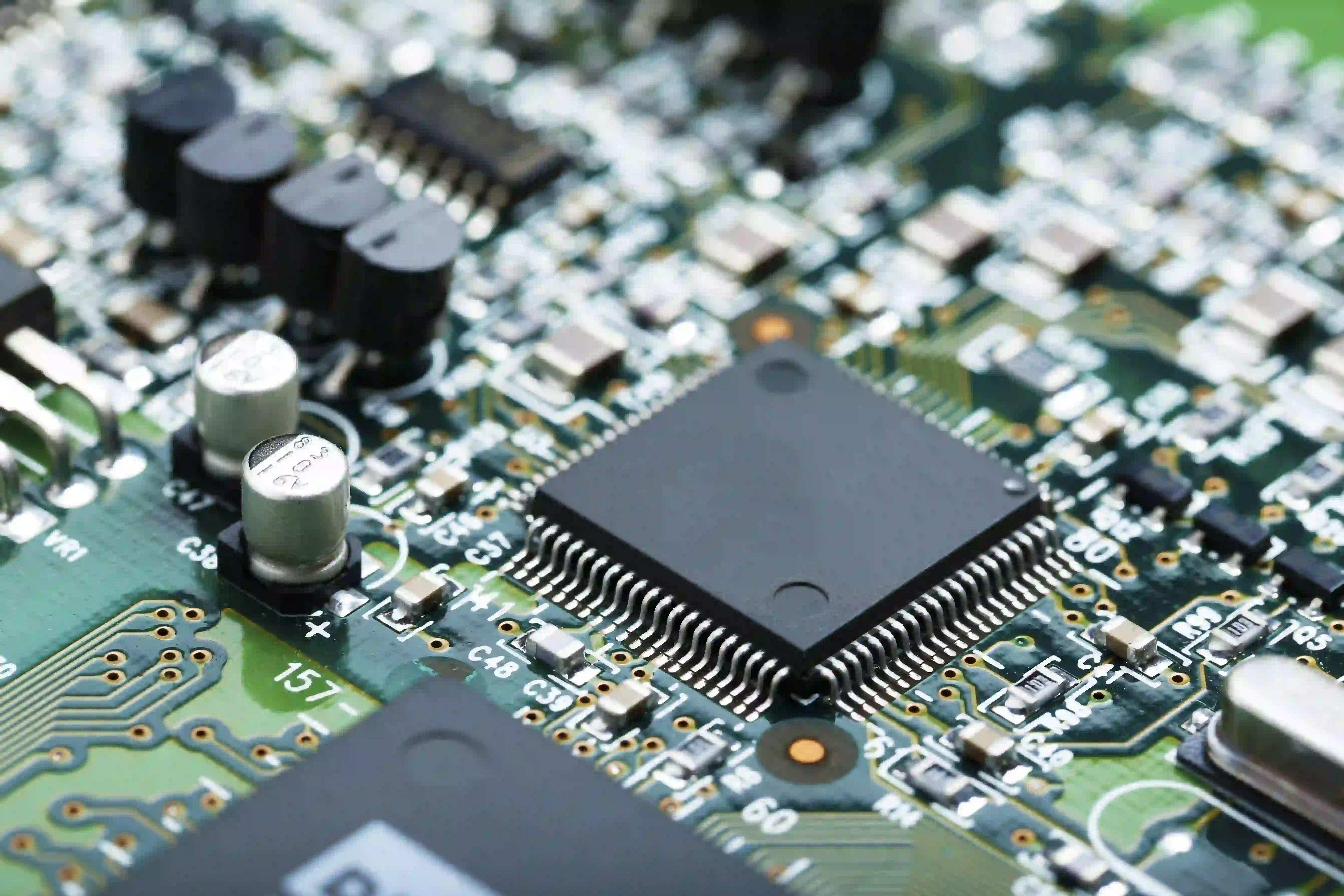
How Stacked Vias Revolutionize PCB Miniaturization
Discover how stacked vias revolutionize PCB miniaturization in HDI designs. This 2026 guide compares stacked vs staggered vias, details aspect ratio rules (<1:1), copper filling requirements, reliability testing, and up to 30% density gains for smartphones, wearables, and 5G modules. Learn design rules, manufacturing best practices, and when to use stacked microvias for BGA fan-out while maintaining signal integrity.
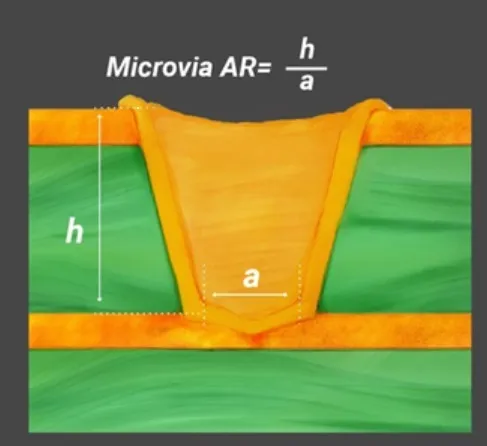
The Impact of Minimum Drill Size on PCB Reliability: Avoiding Manufacturing Defects
Minimum drill size affects pcb drill size reliability through drill wander pcb, pcb hole plating issues, and annular ring requirements. Minimum drill size dfm practices prevent manufacturing defects, ensuring robust PCBs via standards and factory insights for electrical engineers.
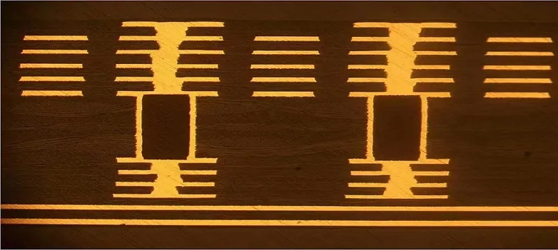
Minimum Drill Size for Microvias: Advanced PCB Design Techniques
PCB microvia drill size sets limits for HDI PCB design density. Laser drilling achieves 50 to 75 micron holes with microvia aspect ratios near 0.8:1. Stacked microvias follow strict rules for reliability. Practical techniques help electrical engineers build high performance boards with better yield.


