Introduction
The PCB manufacturing process transforms a circuit design into a physical printed circuit board that can support electronic components and electrical connections. From consumer electronics to industrial control systems, reliable circuit board manufacturing depends on accurate design data, suitable materials, controlled fabrication, and thorough inspection.
Understanding the printed circuit board manufacturing process helps engineers identify potential production issues before they become costly rework. It also makes it easier to select materials, define manufacturing tolerances, and coordinate PCB fabrication with downstream assembly.
This guide explains the main PCB manufacturing steps, from design preparation and copper patterning to lamination, drilling, surface finishing, and electrical testing. It also covers design for manufacturability (DFM), common production challenges, and the transition from bare-board fabrication to PCB assembly.
Understanding PCB Manufacturing: Fabrication vs. Assembly
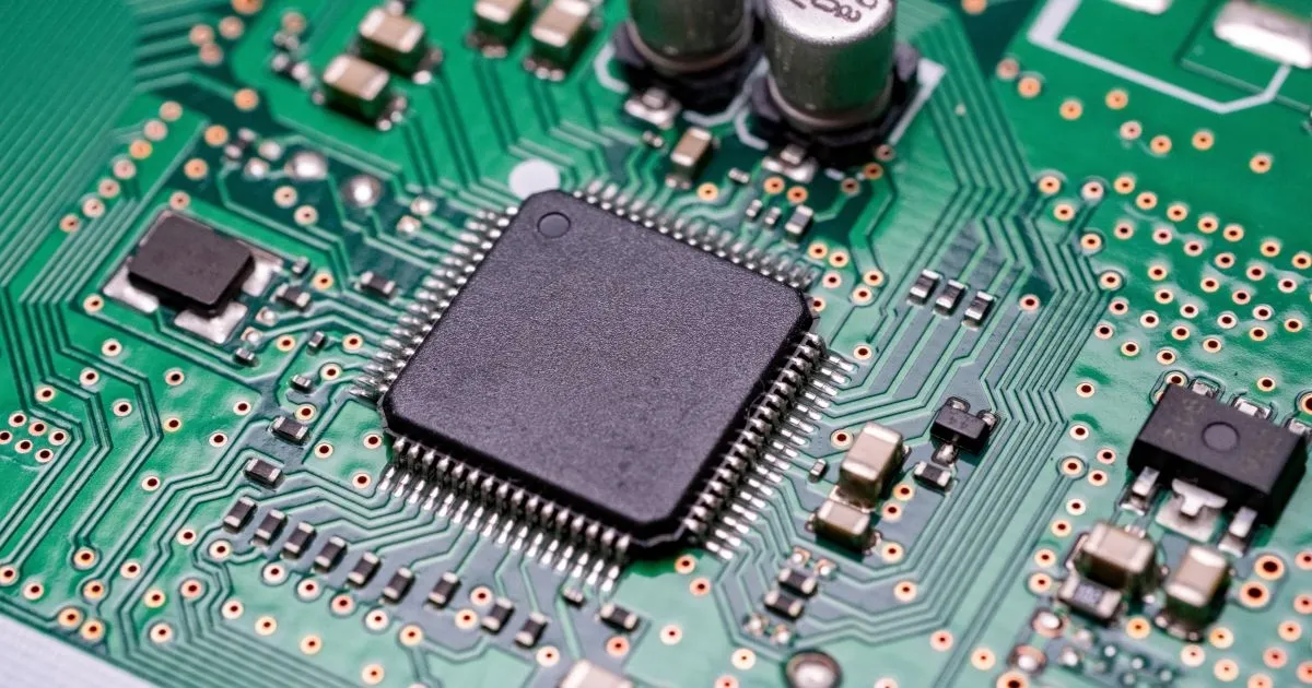
PCB manufacturing encompasses the series of processes involved in creating a functional printed circuit board from a design blueprint. It includes PCB fabrication, which focuses on building the bare board, and PCB assembly, which involves mounting electronic components onto the board. This process is critical because the quality of a PCB directly impacts the performance, reliability, and lifespan of electronic devices. A poorly manufactured PCB can lead to signal integrity issues, thermal failures, or mechanical defects. For electrical engineers, understanding how Cpk process capability is evaluated throughout PCB manufacturing helps ensure that production processes remain consistent, designs are feasible for production, and finished boards meet stringent requirements set by standards like those from IPC and ISO. Monitoring process variation and manufacturing tolerances also supports cost optimization and faster time to market.
The PCB Manufacturing Process Steps

The PCB manufacturing process steps form the core of transforming a design into a functional board. Below, we detail each step sequentially, incorporating technical principles and best practices aligned with industry standards.
Step 1: Design and Data Preparation
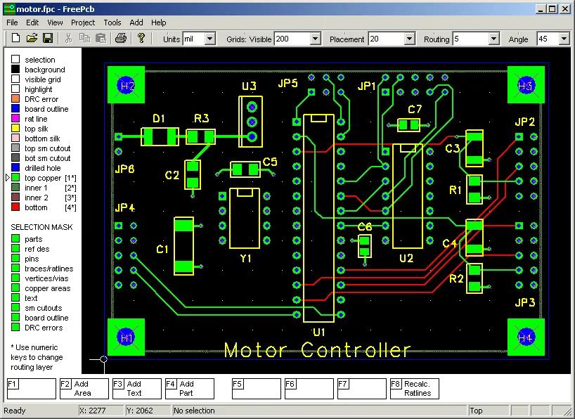
The PCB design and manufacturing process begins with circuit layout and manufacturing documentation. Engineers use electronic design automation (EDA) software to define component placement, copper routing, board outlines, drill locations, layer assignments, and electrical constraints.
Before production, the design data must be checked for completeness and consistency. Manufacturers commonly review Gerber or other accepted fabrication files, drill data, board stackup information, material specifications, copper requirements, and fabrication notes.
A design for manufacturability (DFM) review helps identify potential issues such as insufficient copper spacing, unsuitable drill-to-copper clearance, incomplete solder mask openings, and impractical tolerances. For controlled-impedance designs, engineers should also provide the required impedance values and relevant stackup constraints.
Clear documentation reduces interpretation errors and helps the manufacturer determine whether the design can be produced as specified. Early communication is especially valuable for complex multilayer boards, fine-pitch components, and high-density interconnect (HDI) structures.
Step 2: Inner Layer Fabrication for Multilayer Boards
For multilayer circuit boards, inner layer fabrication begins with copper-clad laminate. A photosensitive resist is applied to the copper surface, and the circuit pattern is transferred using an imaging process.
The resist is developed according to the selected process, defining which copper areas remain protected. Chemical etching then removes unwanted copper, leaving the intended conductive traces and planes.
After etching, the remaining resist is stripped away. Automated optical inspection (AOI) checks the resulting patterns for defects such as unwanted copper connections, missing traces, and pattern deviations.
The accuracy of this stage affects electrical clearance, trace geometry, and the alignment of later layers. Fine-line and HDI designs require particular attention to imaging resolution and etching control.
Step 3: Lamination and Stackup Formation
Once the inner layers have been processed and inspected, multilayer PCBs are assembled into a stack. Copper-clad cores and insulating prepreg materials are arranged according to the specified layer sequence.
Heat and pressure bond the materials into a unified structure. The process must account for resin flow, layer registration, material compatibility, and the board's intended electrical and mechanical performance.
Stackup design affects impedance control, signal return paths, power distribution, and manufacturing complexity. An unsuitable layer arrangement or poorly balanced construction may contribute to warpage, registration problems, or delamination.
Engineers should confirm the layer sequence, dielectric materials, copper weights, and finished board thickness before production. These details help ensure that the fabricated board matches the design requirements.
Related Reading: PCB Stack Up to Plan, Design, Manufacture and Repeat
Step 4: Drilling for Vias and Through-Holes
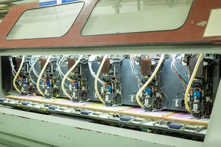
Drilling creates the holes required for electrical connections and component mounting. CNC drilling is commonly used for mechanical holes, plated through-holes, and many via structures. Laser drilling may be used for microvias in suitable HDI designs.
Hole size, position, aspect ratio, and alignment must match the board's design requirements. Drilling errors can affect component fit, plating quality, and electrical continuity.
After drilling, the holes may undergo cleaning and desmear treatment to remove resin residue from the inner copper surfaces. Proper preparation is important because contamination can interfere with the subsequent copper plating process.
Different via structures serve different purposes. Through-holes connect layers through the board, while blind and buried vias connect selected layers according to the stackup. The appropriate structure depends on routing density, electrical requirements, and fabrication capabilities.
Step 5: Copper Plating and Outer Layer Processing
For plated holes, the exposed hole walls must become conductive so that electrical connections can be established between layers. A chemical copper deposition process typically creates an initial conductive layer, followed by electroplating to build the required copper thickness.
The outer copper layers are then patterned using imaging, plating, etching, or other steps appropriate to the selected fabrication process. Unwanted copper is removed, leaving the required traces, pads, and planes.
Process control is important throughout this stage. Inadequate plating, contamination, poor hole preparation, or excessive etching can affect connectivity and trace geometry.
Manufacturers use suitable inspection and verification methods to assess copper features and plated-hole quality. For designs with demanding electrical requirements, the manufacturing specifications should clearly identify the required copper thicknesses and tolerances.
Step 6: Solder Mask Application
Solder mask is the protective coating applied over selected copper areas of a PCB. It helps insulate traces, reduces the risk of solder bridging, and protects exposed circuitry from environmental contamination.
The coating is applied and patterned so that soldering pads and other designated areas remain accessible. The board then undergoes the appropriate exposure, development, and curing operations for the selected solder mask system.
Solder mask registration is important for fine-pitch pads and densely routed boards. Misalignment, pinholes, incomplete coverage, or poor adhesion can compromise protection or interfere with assembly.
The solder mask color is usually a secondary consideration compared with coating suitability, registration, and performance. Engineers should specify any special requirements when appearance, insulation, or operating conditions are critical.
Step 7: Silkscreen Printing
Silkscreen printing adds identifying information to the board, including component reference designators, polarity markings, logos, and other assembly instructions.
The markings may be produced using screen printing or direct legend printing, depending on the manufacturing process. Their position and readability should be checked against the component layout and exposed pad areas.
Although silkscreen is not normally part of the electrical circuit, clear markings help with component placement, inspection, repair, and maintenance. Crowded or incorrectly positioned legends can create confusion during assembly.
Good PCB design therefore balances labeling needs with component clearances and available board space.
Step 8: Surface Finish Selection
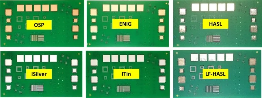
A surface finish protects exposed copper and supports soldering during PCB assembly. The appropriate finish depends on pad geometry, component pitch, storage requirements, assembly processes, and project specifications.
Common options include:
-
HASL: A solder-based finish widely used for suitable general-purpose applications, although its surface may be less uniform than some alternatives.
-
ENIG: Electroless nickel immersion gold provides a relatively flat surface and is often selected for fine-pitch components.
-
Immersion silver: A flat finish that can suit designs requiring good solderability, provided storage and handling are controlled.
-
OSP: An organic protective coating that preserves exposed copper for soldering and requires appropriate handling and assembly conditions.
No single surface finish is ideal for every PCB. Engineers should evaluate component requirements, assembly compatibility, expected storage conditions, and cost before making a selection.
Related Reading: Advanced Surface Finishes: Choosing the Right Option for PCB Mass Production
Step 9: Electrical Testing and Inspection
After fabrication, the board undergoes inspection to verify that it meets the required manufacturing specifications.
Electrical testing commonly checks for unintended shorts and open circuits. Flying-probe testing is useful for many prototype and lower-volume requirements, while fixture-based testing may suit appropriate production runs.
AOI checks visible copper patterns and other inspectable features. Depending on board construction and the inspection plan, additional methods such as X-ray examination or cross-section analysis may be used to evaluate internal structures and plated holes.
Final inspection can also cover board dimensions, hole quality, solder mask, surface finish, and visible defects. The required acceptance criteria should be agreed upon before production rather than assumed to be identical for every project.
These checks complete the core PCB fabrication process and establish whether the bare boards are ready for assembly or delivery.
Best Practices for Reliable PCB Production
Optimizing Design for Manufacturability
A DFM review should identify potential issues before fabrication begins. Check trace widths and spacing, hole sizes, annular rings, copper clearances, board edges, solder mask openings, and layer registration against the selected manufacturer's capabilities.
Design requirements should reflect the actual electrical and mechanical needs of the project. Avoid specifying unnecessarily tight tolerances when they do not improve performance, but do not relax critical requirements without engineering review.
Material Selection for Reliability
Material selection affects dielectric behavior, thermal performance, mechanical stability, and cost. Standard FR-4 may suit many general-purpose applications, while high-frequency, high-temperature, or specialized products may require other materials.
The material should be selected according to the operating environment and electrical requirements rather than by price alone. Confirm that the manufacturer can process the selected material and stackup reliably.
Managing PCB Etching Precision
Managing PCB etching precision involves monitoring chemical baths to prevent under- or over-etching; for HDI boards, laser etching can achieve finer traces down to 50 microns. IPC-6012E guidelines ensure uniformity.
Related Reading: Advanced PCB Etching Techniques for High Density Interconnect (HDI) Boards
Streamlining PCB Assembly Processes
Streamlining PCB assembly uses SMT for efficiency, with solder paste stenciling followed by reflow at profiles per JEDEC J-STD-020E to avoid thermal damage. Automated inspection post-assembly confirms joint quality.
Troubleshooting Common Manufacturing Issues
Addressing Drilling Misalignment
Drilling misalignment can disrupt via connectivity, leading to electrical failures. This often stems from improper machine calibration or material warpage. Engineers should specify tight tolerances in design files and verify fabricator capabilities. Post-drilling inspection per IPC-6012E standards helps identify and rectify issues early.
Correcting Solder Mask Defects
Solder mask defects, such as incomplete coverage or pinholes, expose copper to oxidation. This may result from uneven application or curing issues. Adjusting exposure parameters and ensuring cleanliness during application resolves most problems. Referencing IPC-SM-840E aids in defining acceptable defect levels.
Related Reading: Solder Mask Misalignment: Causes, Consequences, and Solutions for Robust PCB Production
Preventing Surface Finish Inconsistencies
Inconsistent surface finish can hinder solderability or cause reliability issues. Variations in plating thickness or contamination are common culprits. Strict process controls and adherence to JEDEC J-STD-609A during application ensure uniform finish quality across batches.
Conclusion
The PCB manufacturing process is a complex sequence of steps that transforms design concepts into functional boards. From initial data preparation to final surface finish application, each stage demands precision and adherence to industry standards like those from IPC and JEDEC. Electrical engineers who understand PCB fabrication, etching, drilling, and assembly can better optimize designs for reliability and cost efficiency. By focusing on material selection, process control, and thorough inspection, potential issues can be minimized. This guide serves as a foundation for navigating the intricacies of PCB production, ensuring high-quality outcomes for diverse applications.
FAQs
Q1: How does PCB etching impact the quality of a printed circuit board?
A1: PCB etching directly affects trace accuracy and electrical performance. If not controlled, over-etching can thin traces, increasing resistance, while under-etching may leave unwanted copper, risking shorts. Following standards like IPC-6012E ensures precise removal of excess copper. Proper chemical monitoring and process adjustments are essential for consistent results, especially in high-density designs.
Q2: What factors should engineers consider during PCB drilling?
A2: During PCB drilling, engineers must consider hole size, placement accuracy, and material properties. Misaligned or oversized holes can disrupt connectivity in vias or through-hole components. Specifying tolerances as per IPC-6012E and selecting appropriate drill speeds prevent defects. Material warpage should also be minimized to maintain precision across the board.
Q3: Why is solder mask application critical in PCB manufacturing?
A3: Solder mask application protects copper traces from oxidation and prevents short circuits during assembly. It ensures only designated pads are exposed for soldering, enhancing reliability. Defects like pinholes can compromise this protection. Adhering to IPC-SM-840E standards during application guarantees durability and performance under various environmental conditions.
Q4: How does surface finish selection influence PCB assembly outcomes?
A4: Surface finish selection impacts solderability and long-term reliability in PCB assembly. Finishes like ENIG offer excellent corrosion resistance, while HASL is cost-effective but less uniform. Choosing the right finish per JEDEC J-STD-609A ensures compatibility with soldering processes and environmental stresses. This decision affects both assembly quality and product lifespan.
Q4: Is PCB manufacturing suitable for both prototypes and high-volume orders?
A4: Yes. PCB manufacturers may support prototype, small-batch, and larger production orders, depending on their equipment and production capabilities. Prototype orders help validate a design, while higher-volume production places greater emphasis on repeatability, process consistency, and production planning. The appropriate supplier should match the project's volume and technical requirements.
Q5: What information should be confirmed before choosing a PCB manufacturing supplier?
A5: Beyond the quoted price, consider the supplier's experience with the required board type, available fabrication capabilities, quality documentation, communication process, and ability to support future production needs. If the project includes assembly, confirm whether component sourcing, assembly, and testing are available as part of the service or must be arranged separately.
Q6: Can PCB manufacturing requirements change between different applications?
A6: Yes. Consumer electronics, industrial controls, automotive systems, telecommunications equipment, and other applications can have different electrical, mechanical, thermal, and reliability requirements. These differences may influence board construction, material selection, inspection criteria, and documentation. Manufacturing requirements should therefore be defined according to the intended operating environment and applicable product specifications.
References
IPC-2221B — Generic Standard on Printed Board Design. IPC, 2012.
IPC-6012E — Qualification and Performance Specification for Rigid Printed Boards. IPC, 2020.
IPC-A-600K — Acceptability of Printed Boards. IPC, 2020.
IPC-SM-840E — Qualification and Performance of Permanent Solder Mask and Flexible Cover Materials. IPC, 2011.
IPC-4101E — Specification for Base Materials for Rigid and Multilayer Printed Boards. IPC, 2017.
JEDEC J-STD-020E — Moisture/Reflow Sensitivity Classification for Nonhermetic Surface Mount Devices. JEDEC, 2014.
JEDEC J-STD-609A — Marking and Labeling of Components, PCBs and PCBAs to Identify Lead (Pb), Lead-Free (Pb-Free) and Other Attributes. JEDEC, 2011.