500W Lead-Acid Battery Charging System
Technical design of a 50V battery charger covering EMI filtering, PFC boost, full-bridge DC-DC stage, control/protection, thermal monitoring, and four-stage charging strategy.
Power and new energy solutions represent a critical frontier in modern electronics, where innovative PCB designs drive efficiency, sustainability, and performance across diverse applications. In this Power & New Energy Solutions category, we delve into the technologies shaping the future of energy management, from advanced power supplies and renewable energy systems to smart grid integrations and energy storage solutions. Our focus extends to the intricate role of printed circuit boards in optimizing power distribution, minimizing losses, and enabling seamless integration with emerging energy sources like solar, wind, and electric vehicles. Professionals in electronics engineering and PCB design will find valuable resources here, including detailed guides on selecting components for high-efficiency power converters, tutorials on implementing energy-harvesting techniques, and insights into regulatory standards for sustainable energy projects. We also share best practices for thermal management in power-intensive applications, ensuring reliability in demanding environments such as industrial automation and automotive electrification. The practical value of these topics lies in their direct impact on real-world challenges, such as reducing carbon footprints through efficient energy use or enhancing battery life in portable devices. By addressing both foundational concepts and cutting-edge advancements, our content equips readers with the knowledge to tackle complex projects and innovate in a rapidly evolving field. As you browse the articles in this category, you'll uncover strategies to improve system performance, navigate design trade-offs, and stay ahead of industry trends, fostering informed decisions that advance your work in power and energy technologies.
Technical design of a 50V battery charger covering EMI filtering, PFC boost, full-bridge DC-DC stage, control/protection, thermal monitoring, and four-stage charging strategy.
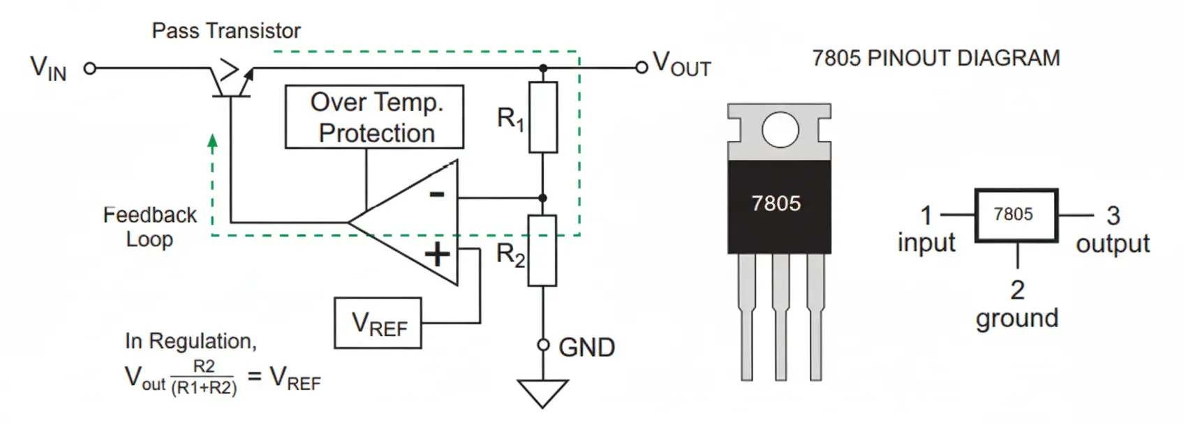
Technical overview of linear regulators, explaining closed-loop operation, feedback control, efficiency trade-offs, and low-dropout (LDO) design, with advantages and applications.
AC peak detector design for over/undervoltage protection: analyzes filter-induced timing lag and a phase-lag compensation method to restore correct peak readings.
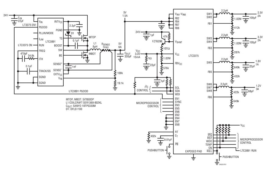
Discover the LTC3375 multi-output synchronous buck converter for industrial electronics. Learn about configurable 1A-4A outputs, I2C control, power sequencing, watchdog timer, and key PCB layout considerations for reliable power distribution in complex systems.
Technical overview of portable power stations, market growth, DC-DC/DC-AC topologies and MOSFET selection guidance for portable energy storage designs.
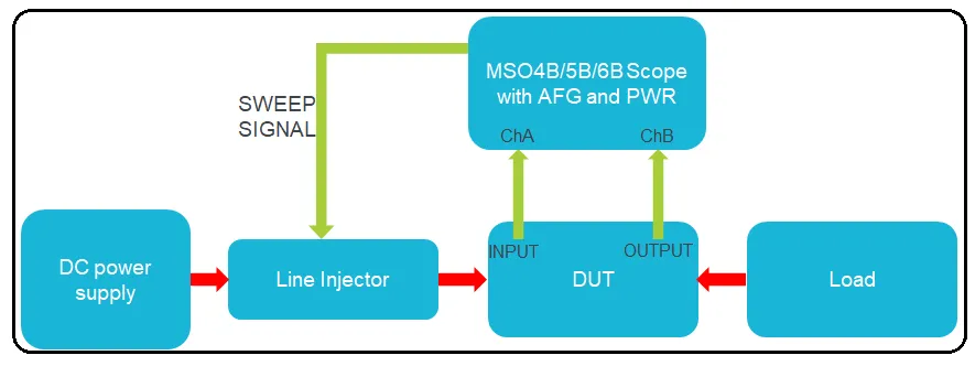
PSRR measurement guide covering power supply rejection ratio theory, test methods, and recommended oscilloscope-based setup, equipment, and validation procedures.
Explore radioisotope thermoelectric generators (RTGs) and nuclear batteries for aerospace, medical, and harsh-environment applications. Learn about decay heat conversion, thermoelectric materials, radiation shielding, and the role of high-reliability PCBs in power management and system integration.
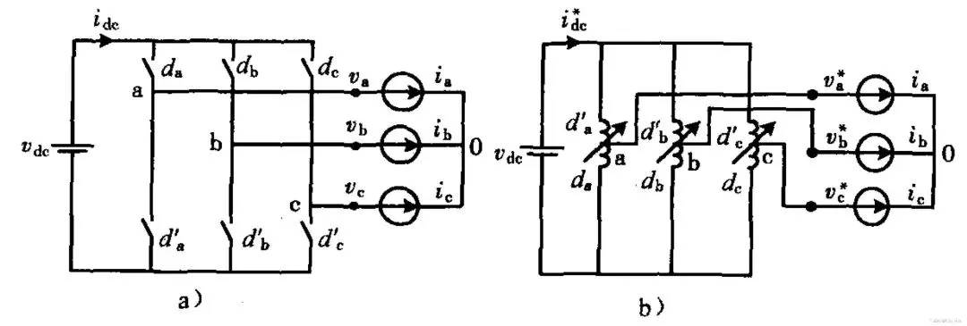
Technical overview of three-phase inverter modeling: circuit topology, abc/alpha-beta/dq-frame mathematical models using Clarke and Park transforms for controller design.
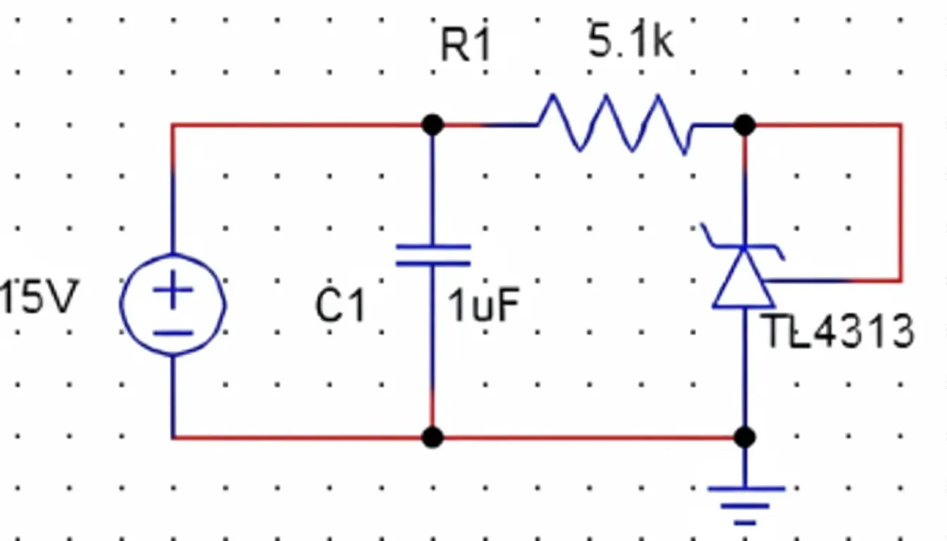
Review of constant-current source topologies: op-amp with TL431 reference, two-NPN Vbe current source, and TL431-plus-transistor design with analysis and simulations.
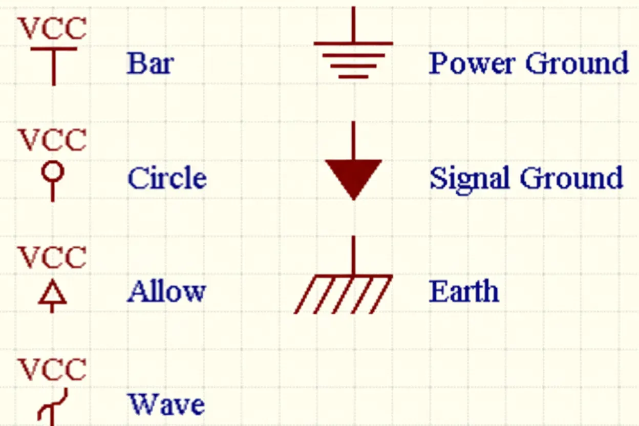
Learn essential strategies for protective earthing and neutral paths in PCB power design. This overview details ground resistance, voltage regulators, and transformers for safe, reliable electronics.
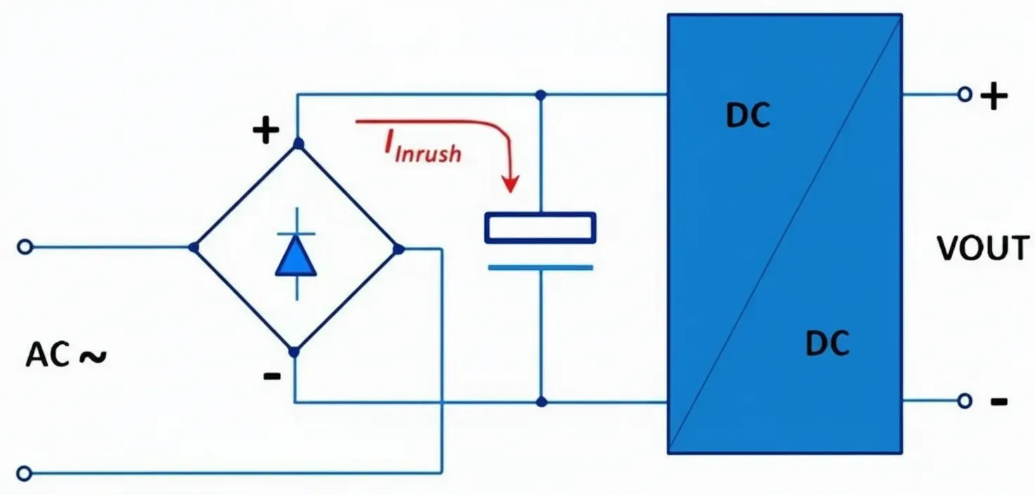
Six practical methods to reduce start-up inrush current in SMPS, including NTC/PTC thermistors, series resistors, SCR bypass, and controlled MOSFET switching.
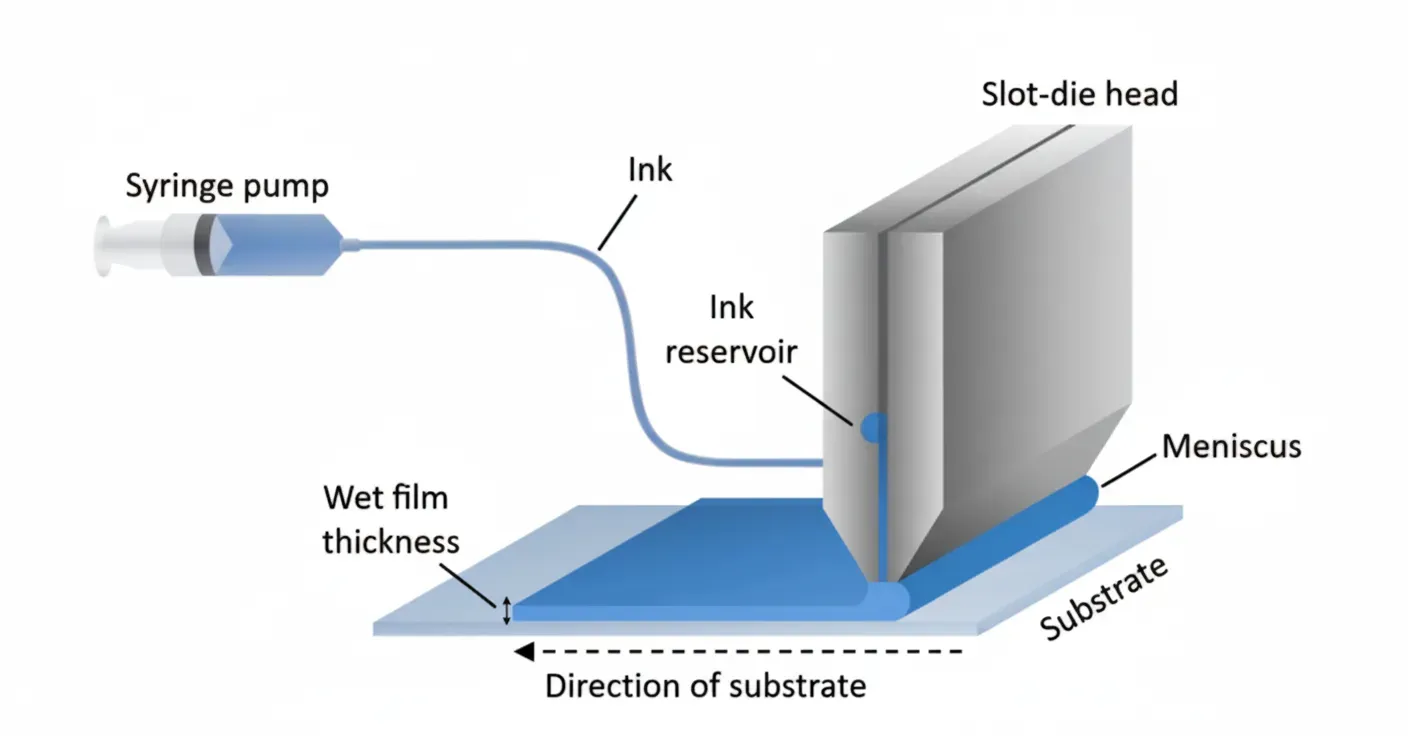
Slot-die coating overview, principles, advantages, limitations and scalability for thin films; covers small-scale tools, roll-to-roll integration and thickness control.