High-Speed PCB
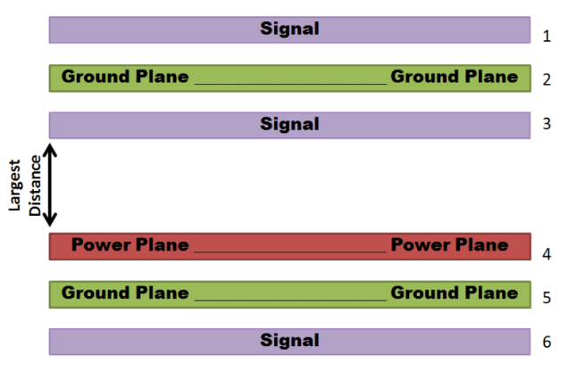
High-speed printed circuit boards (PCBs) are essential components in modern electronics, enabling the reliable transmission of signals at frequencies exceeding 100 MHz. These specialized boards address the challenges of signal integrity, electromagnetic interference, and thermal management in applications such as telecommunications, data centers, automotive systems, and high-performance computing. For engineers and designers searching for High-Speed PCB resources, this tag serves as a comprehensive hub, offering in-depth guidance on optimizing designs to prevent issues like crosstalk, reflections, and timing errors that can degrade performance. Understanding the fundamentals of high-speed PCB design begins with selecting appropriate materials, such as low-loss dielectrics and controlled-impedance traces, to maintain signal quality over long distances. Best practices include implementing proper layer stacking for multilayer boards, using differential signaling to reduce noise, and incorporating ground planes to minimize EMI. Practical applications often involve simulation tools like SPICE or electromagnetic field solvers to predict and mitigate potential problems before prototyping, saving time and costs in the development cycle. For instance, in 5G infrastructure, high-speed PCBs ensure seamless data transfer rates, while in consumer electronics, they support faster processing in devices like smartphones and gaming consoles. Professionals tackling high-speed projects can benefit from actionable insights on via optimization, such as back-drilling to eliminate stubs, and routing techniques that prioritize signal path length matching. This collection of articles explores these topics through real-world examples and case studies, helping you apply proven strategies to your own designs. Whether you are refining an existing layout or starting a new high-frequency project, the resources here provide the technical depth needed to achieve robust, efficient results.
Technical Articles
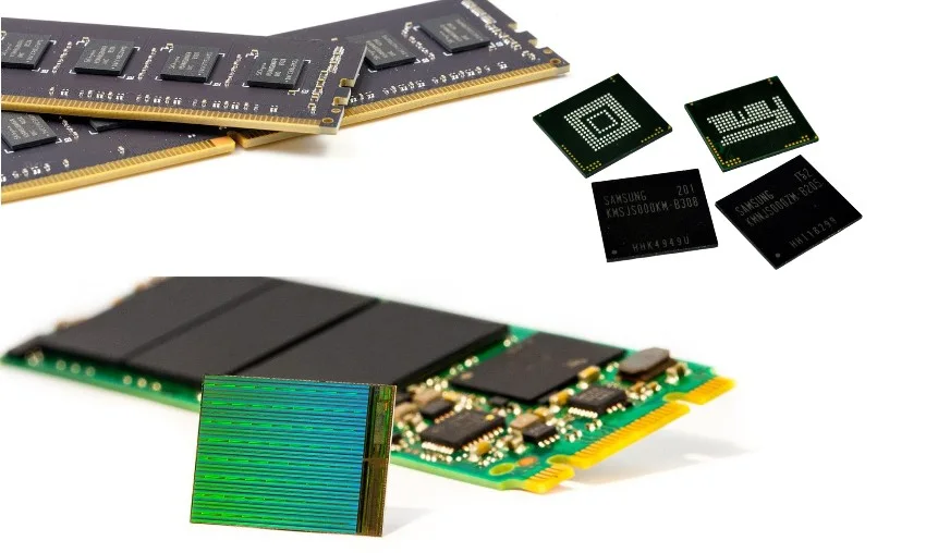
Selecting Memory Types for In-Memory Computing Chips

Single 1TB Memory Module Appears Achievable
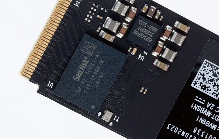
PCIe SSD PCB Design: 3D NAND Scaling, High-Speed Interfaces, QLC Endurance, and Automotive Storage Solutions
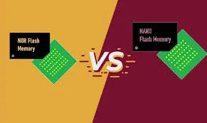
NAND vs NOR Flash Memory in PCB Design: Technical Comparison, Interface Selection, and Optimization Strategies
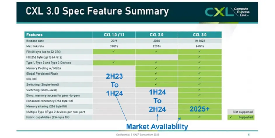
Memory Interface Chip Technologies Overview
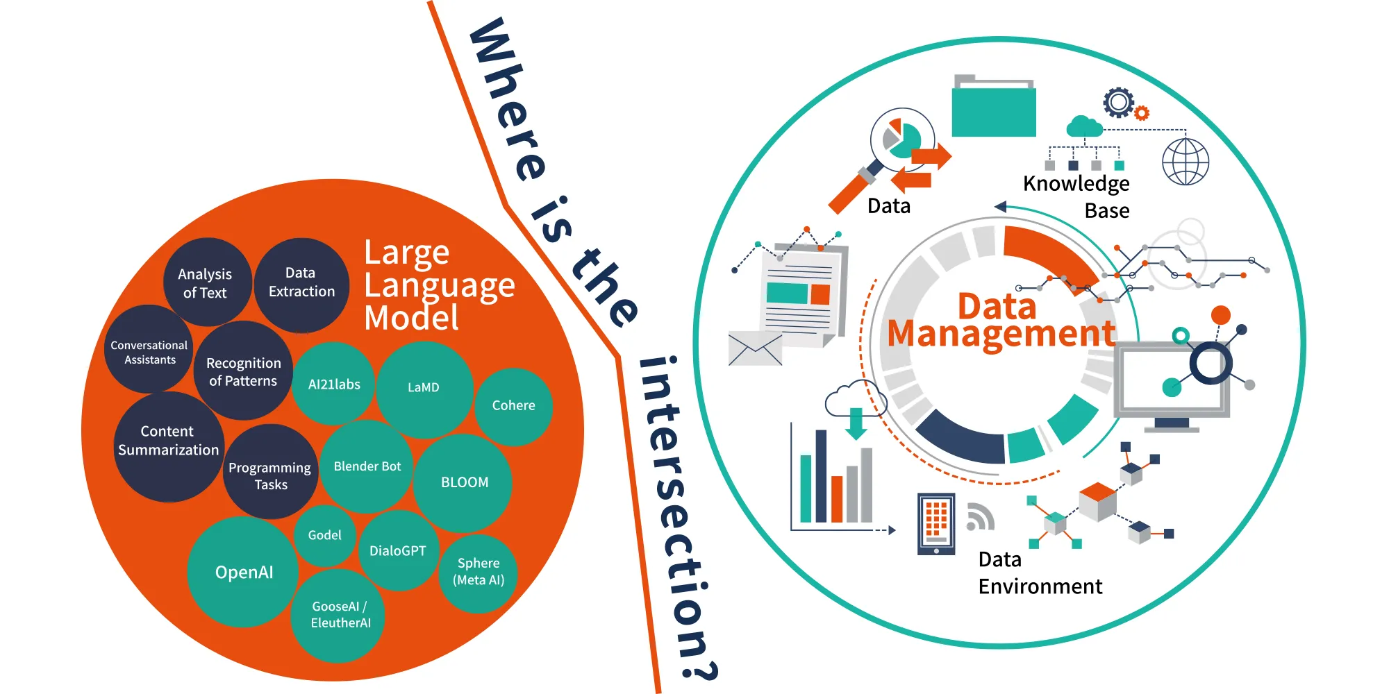
How Large Language Models Impact Data Storage
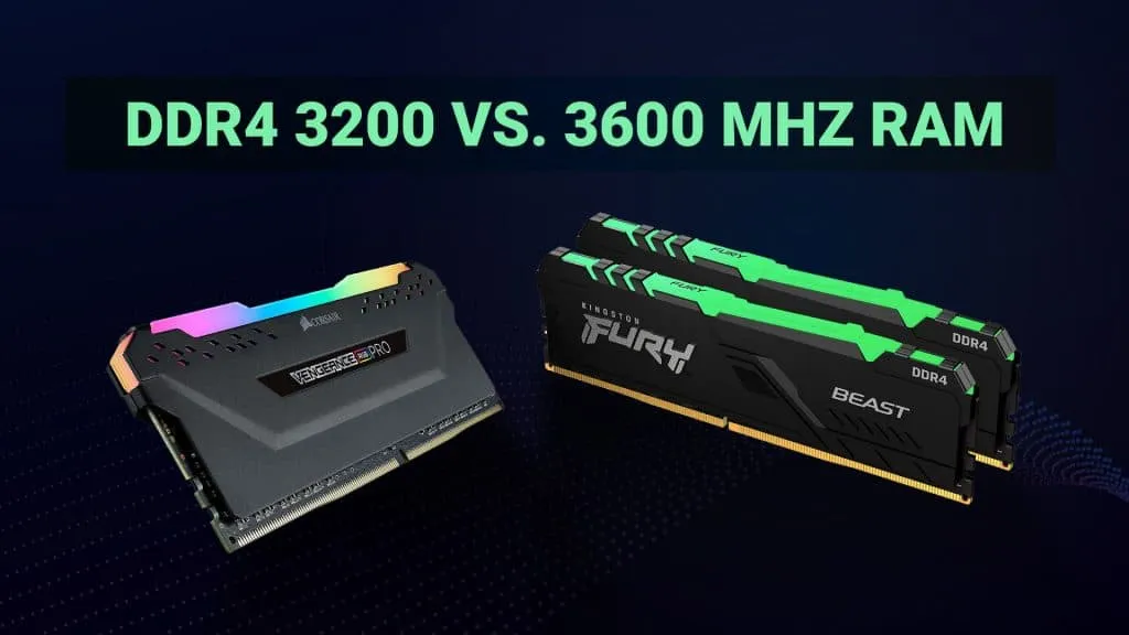
DDR4 3200 vs 3600: Differences and Compatibility
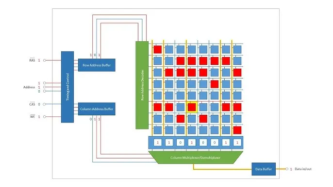
DRAM vs SRAM and DDR Memory Generations in PCB Design: Architecture, Signal Integrity, Bandwidth Optimization, and Manufacturing Guidelines
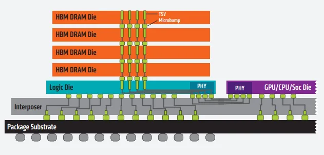
Choosing the Right Memory Technology for PCB Designs: Engineering Considerations for Performance, Reliability, and Manufacturability
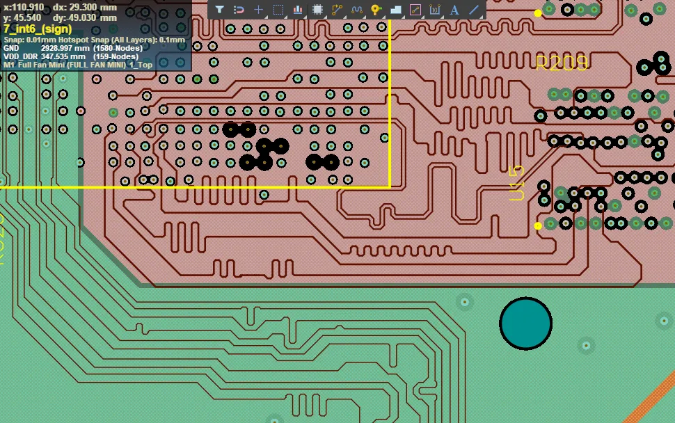
Troubleshooting Signal Integrity Issues in High Speed PCBs: A Practical Guide
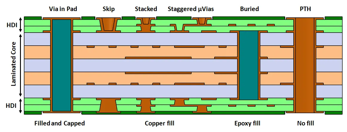
The Role of PCB Materials in High Speed Design: Choosing the Right Dielectric
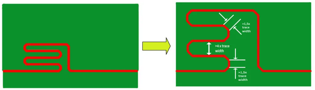
Component Placement Strategies for High Speed PCBs: Reducing EMI and Signal Loss

Memory Technologies in New Flagship Smartphones
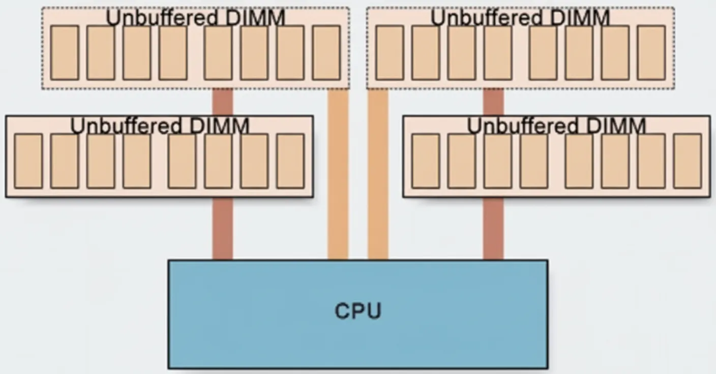
DDR3 and DDR4 Memory: Technical Notes
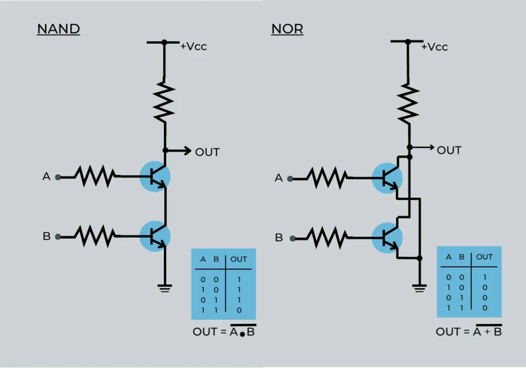
NOR and NAND Flash Application Circuits
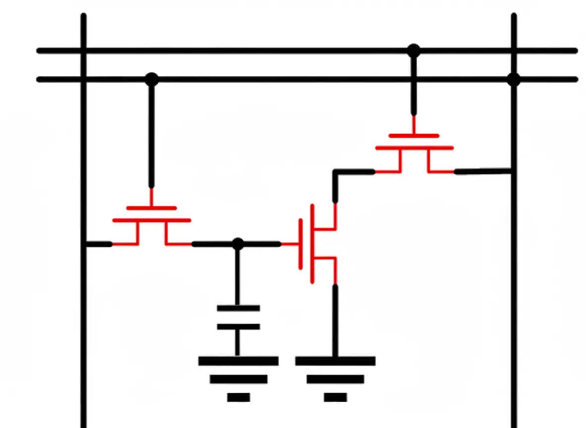
How DRAM Stores and Reads Data
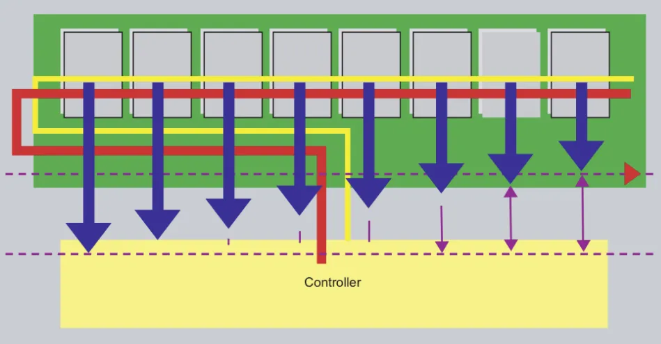
DDR3 Bandwidth Calculation
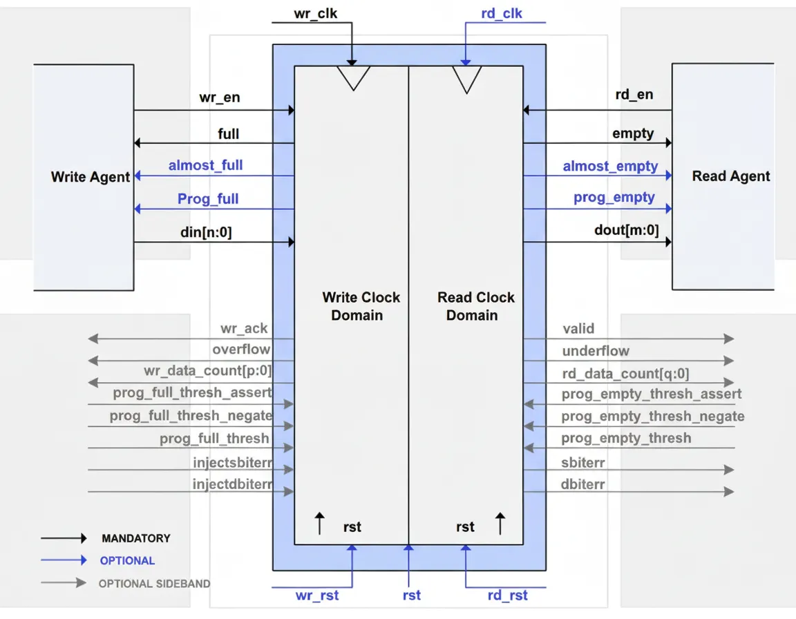
BRAM Basics for FPGA Design