02:50
02:50
PCB Filled Vias
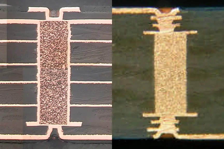
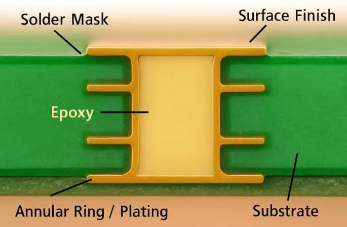
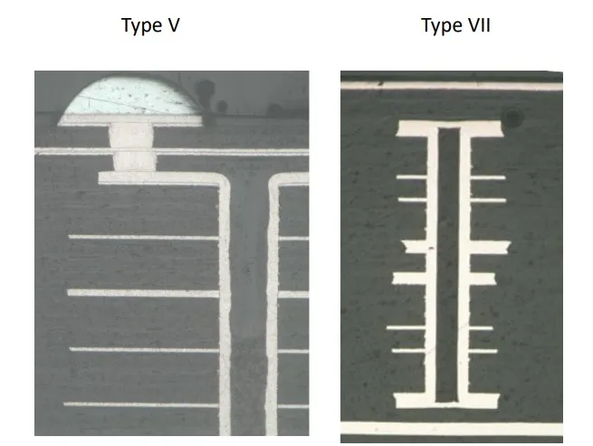
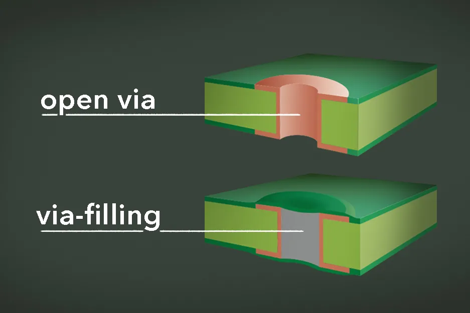
PCB filled vias represent a critical advancement in printed circuit board design, offering enhanced reliability and performance for multilayer boards. These vias are essentially through-holes or blind vias that are filled with conductive or non-conductive materials, such as epoxy or copper, to prevent issues like solder wicking, voids, or structural weaknesses. For engineers and designers searching for information on PCB filled vias, this tag serves as a comprehensive resource, covering everything from basic implementation to advanced techniques that optimize signal integrity and thermal management in high-density interconnects. Understanding the practical applications of PCB filled vias can significantly improve your PCB projects. In high-speed electronics, filled vias reduce parasitic inductance and capacitance, ensuring cleaner signal transmission. They are particularly useful in via-in-pad designs, where components are mounted directly over vias to save space on compact boards like those in smartphones or automotive systems. Best practices include selecting the appropriate fill material based on your board's requirements; for instance, conductive fills excel in heat dissipation for power electronics, while non-conductive options provide better insulation in sensitive RF applications. Proper filling also minimizes manufacturing defects, such as dimpling or overfill, which can be addressed through precise process controls like tenting or planarization. If you are troubleshooting common challenges or seeking design guidelines, the articles grouped under this tag delve into real-world examples and step-by-step tutorials. From comparing filled vias to traditional tented vias to exploring their role in HDI PCBs, these resources equip you with actionable insights to elevate your designs. Whether you are a seasoned PCB engineer or just starting out, reviewing these topics can help you make informed decisions that enhance board durability and functionality.
Video Guide
-
02:50
Technical Articles