00:52
PCB Gold Fingers
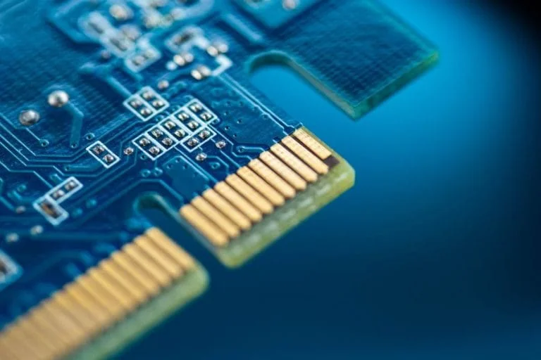
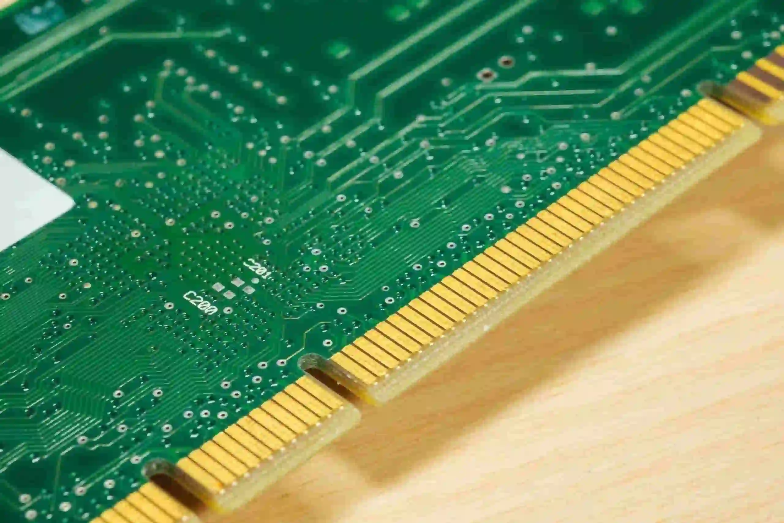
PCB gold fingers refer to the gold-plated edge connectors on printed circuit boards that facilitate reliable electrical connections in devices such as computer motherboards, graphics cards, and expansion modules. These specialized contacts are essential for ensuring high conductivity, corrosion resistance, and durability in high-performance electronics, where repeated insertions and removals demand robust materials. Gold plating minimizes oxidation and wear, providing a stable interface that supports data transfer rates and signal integrity in demanding environments like servers and consumer gadgets. For engineers and designers searching for information on PCB gold fingers, this tag aggregates articles that delve into key aspects of their implementation. You will find guidance on selecting appropriate gold thickness to balance cost and performance, typically ranging from 30 to 50 microinches for optimal results. Practical applications include edge connectors in PCIe slots or DIMM modules, where precise alignment and beveling prevent misalignment during assembly. Best practices emphasize proper PCB layout to avoid signal crosstalk, incorporating features like chamfered edges and controlled impedance for enhanced reliability. Common challenges, such as plating defects or contamination, are addressed through insights on manufacturing processes like electroless nickel immersion gold (ENIG) and rigorous quality testing. By understanding these elements, you can optimize designs to meet industry standards like IPC-6012, reducing failure rates in production. Articles linked under this tag offer detailed case studies and troubleshooting tips, helping you apply these concepts to your projects effectively. Whether you are prototyping a new board or refining an existing one, the resources here provide the technical depth needed to achieve superior connectivity and longevity in your PCB designs.
Video Guide
-
00:52
Technical Articles
PCB Reliability Testing for SMT: Methods, Criteria, and Process Controls

ENIG "Black Pad" and BGA Solder Reliability: Failure Mechanism, Process Controls, and Acceptance Criteria

Risks of Etching a PCB After ENIG and Thick Gold Finger Plating

Why Do PCBs Use Staggered Gold Fingers?

Why Do Optical Module PCBs Use ENEPIG Surface Finish?

PCB Gold Finger Durability: Insertion-Cycle Guidelines and Wear Factors

Why Gold-Finger Side Copper Exposure Matters on Optical Module PCBs

Why Bonding Finger Roughness Must Be Controlled on Optical Module PCBs
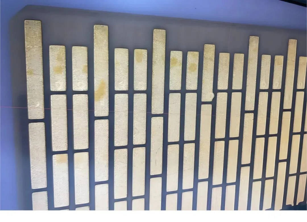
Why Do Optical Modules Use Segmented Gold Fingers?
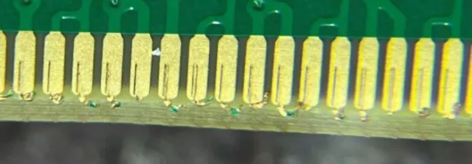
Manufacturing Improvements to Prevent Lifting and Residual Shorts in PCB Gold-Finger Plating Leads
Resolving PCB Gold Finger Plating Problems: A Comprehensive Guide

Gold Bonding Wire in Semiconductor Packages

How to Address Discoloration and Oxidation on PCB Gold Fingers

How to Prevent Gold-Finger Plating Leads from Lifting

ENIG, Electroplated Gold, ENEPIG, and Flash Gold: What Are the Differences?

Is the Nickel in Thick Gold Plating the Same as the Nickel in ENIG?

Can Solder on PCB Gold Fingers Be Accepted?

CAM Review of a 4-Layer FPC: Stiffener Adjustments, Gold Finger Thickness, and Surface Finish Optimization

How Thin Can Gold Finger Plating Be Before Reliability Suffers?