 00:52
PCB Layout
PCB layout forms the backbone of effective electronics design, determining how components are arranged, traces are routed, and signals are managed on a printed circuit board. For engineers, hobbyists, and professionals searching for PCB layout resources, this tag serves as a comprehensive hub for understanding the principles that ensure reliable performance, minimize noise, and optimize space. Whether you are tackling high-speed digital circuits or power electronics, mastering PCB layout techniques can prevent common issues like electromagnetic interference, thermal hotspots, and signal integrity problems, ultimately leading to more robust and efficient prototypes. In practice, effective PCB layout involves strategic decisions such as layer stacking, component placement, and ground plane implementation. For instance, prioritizing short trace lengths for critical signals reduces latency and crosstalk, while incorporating vias judiciously enhances connectivity without compromising board integrity. Best practices also emphasize simulation tools to predict behavior before fabrication, saving time and costs in iterative designs. Users often seek guidance on software like Altium Designer or KiCad, where layout rules can be automated to adhere to manufacturing constraints, ensuring designs are both functional and producible. Articles under this PCB layout tag delve into real-world applications, from automotive electronics to IoT devices, offering step-by-step tutorials on routing strategies and error troubleshooting. By exploring these resources, you can gain insights into advanced topics like differential pair routing or impedance matching, equipping you with the knowledge to elevate your projects. This collection addresses common challenges faced by designers, providing practical solutions that align with industry standards and foster innovation in electronics development.
Video Guide


Technical Articles

The Importance of Choosing the Right PCB Layout Software

PCB Layout Best Practices for Robust Designs
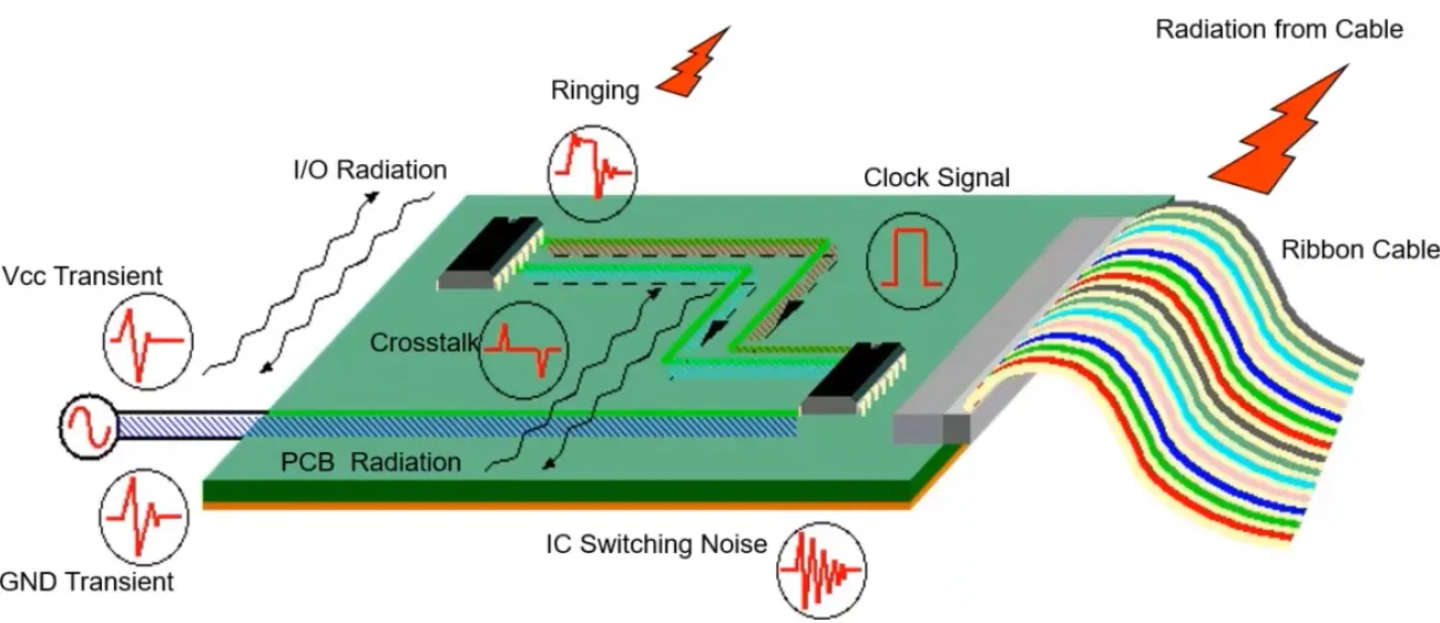
EMI and EMC Compliance 101 for PCB Designers

Fan Microstrip Structures in RF Amplifiers
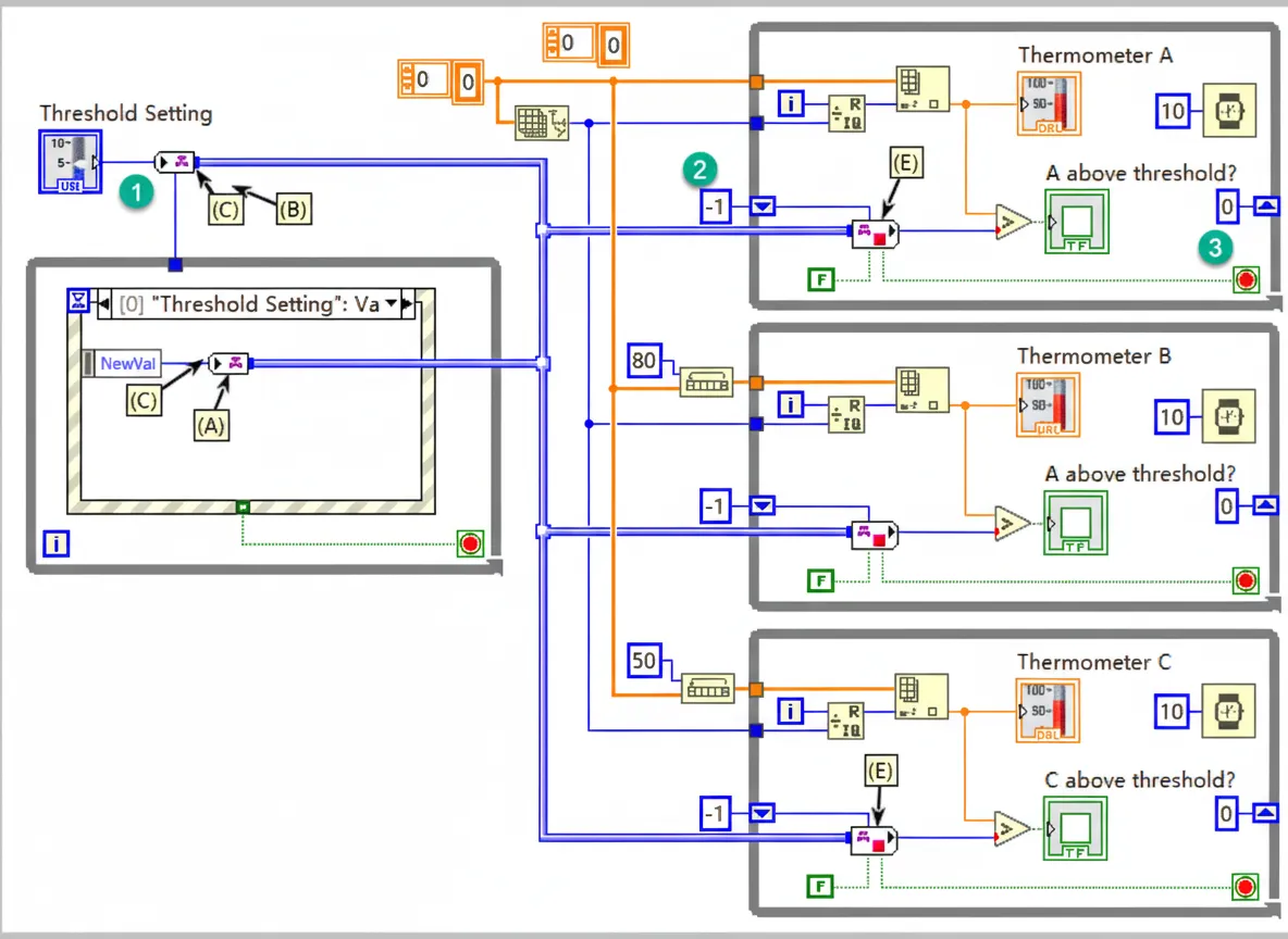
LabVIEW Channel Wire Usage and Caveats

Designing an EEPROM I2C Driver

NAND vs NOR Flash: Technical Comparison

SRAM Basic Circuits and Operating Principles
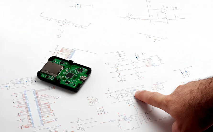
From Napkin Sketch to Gerber File: A Beginner's Guide to PCB Schematic Design

Optimize PCB Design for Small Electronics
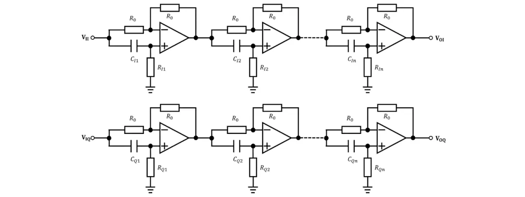
Passive Analog Filters: Two 90° Phase-Shift Networks
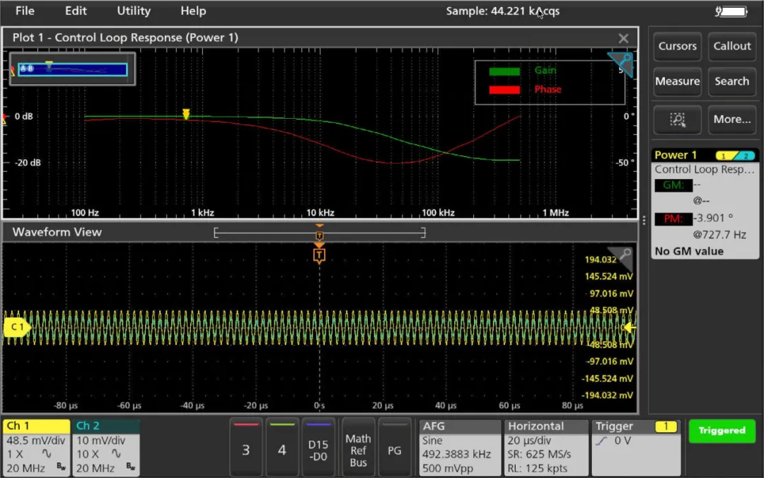
Frequency Response Analysis with an Oscilloscope
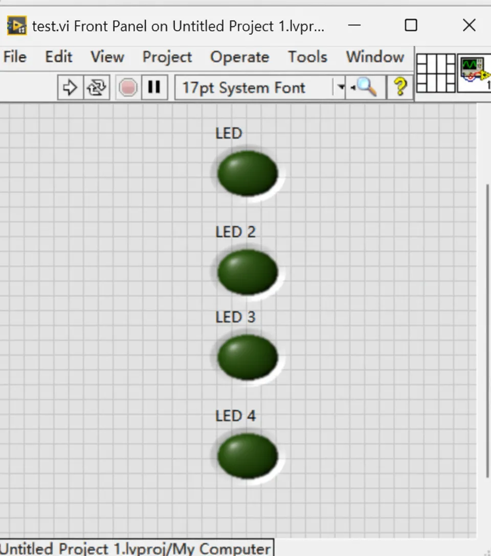
How to Read Command-Line Arguments in LabVIEW Executables

Water Level Measurement Circuit

Principles of Structured-Light Phase Unwrapping
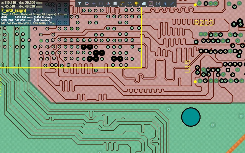
Mastering PCB Layout: Top 10 Common Mistakes and How to Avoid Them
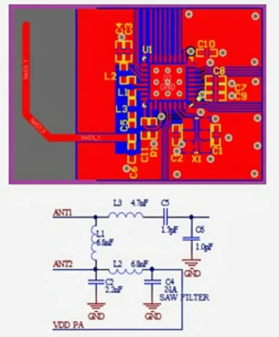
Designing a Smart Wristband with nRF51822

Quantum-Enhanced Network Security
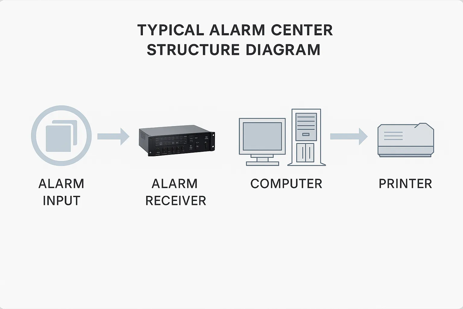
Intrusion Alarm System Design and Applications