










 00:52
00:52
PCB Layout
PCB layout forms the backbone of effective electronics design, determining how components are arranged, traces are routed, and signals are managed on a printed circuit board. For engineers, hobbyists, and professionals searching for PCB layout resources, this tag serves as a comprehensive hub for understanding the principles that ensure reliable performance, minimize noise, and optimize space. Whether you are tackling high-speed digital circuits or power electronics, mastering PCB layout techniques can prevent common issues like electromagnetic interference, thermal hotspots, and signal integrity problems, ultimately leading to more robust and efficient prototypes. In practice, effective PCB layout involves strategic decisions such as layer stacking, component placement, and ground plane implementation. For instance, prioritizing short trace lengths for critical signals reduces latency and crosstalk, while incorporating vias judiciously enhances connectivity without compromising board integrity. Best practices also emphasize simulation tools to predict behavior before fabrication, saving time and costs in iterative designs. Users often seek guidance on software like Altium Designer or KiCad, where layout rules can be automated to adhere to manufacturing constraints, ensuring designs are both functional and producible. Articles under this PCB layout tag delve into real-world applications, from automotive electronics to IoT devices, offering step-by-step tutorials on routing strategies and error troubleshooting. By exploring these resources, you can gain insights into advanced topics like differential pair routing or impedance matching, equipping you with the knowledge to elevate your projects. This collection addresses common challenges faced by designers, providing practical solutions that align with industry standards and foster innovation in electronics development.
Video Guide


Technical Articles
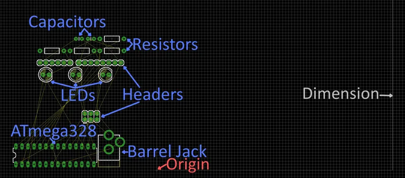
Stuck on PCB Placement? First Arrange These Four Types of Positions
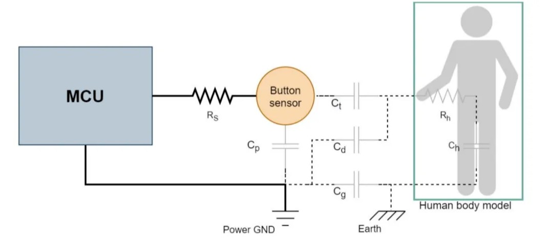
Fundamentals and Principles of Capacitive Touch

Why Power Planes Are Set Back in Multilayer PCB Design: The 20H Rule Explained
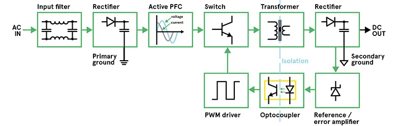
Twelve Switching Power Supply Topologies and How to Calculate Them
Summary | 7 Key Points in PCB Power Design

Classic BJT Switching Circuits: Inverting, Non-Inverting, and Filtering Behavior (Illustrated)
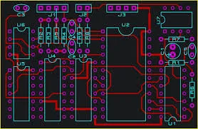
PCB Layout Design Essentials and Practical Techniques
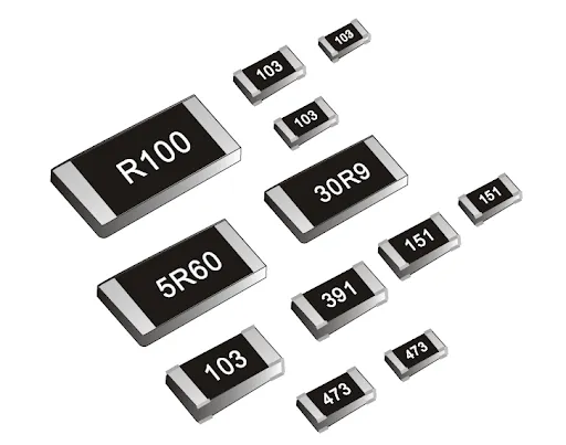
SMD Resistor Codes and Resistance Value Calculations
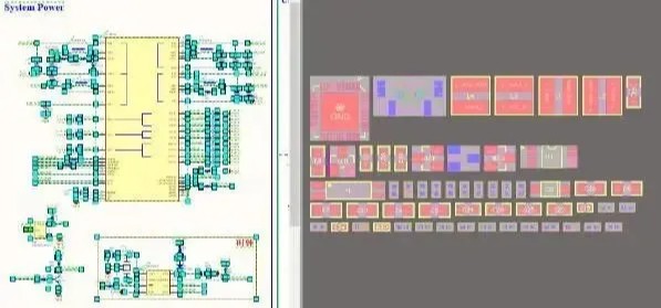
Interactive and Modular PCB Layouts to Double Design Efficiency
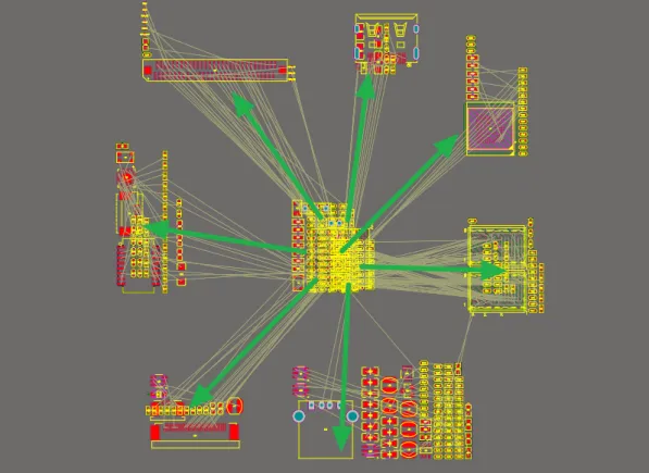
Standard PCB Design Workflow for Engineers
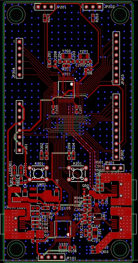
Will AI Replace PCB Engineers?

Can't Do PCB Layout? This Step-by-Step Guide Makes It Simple
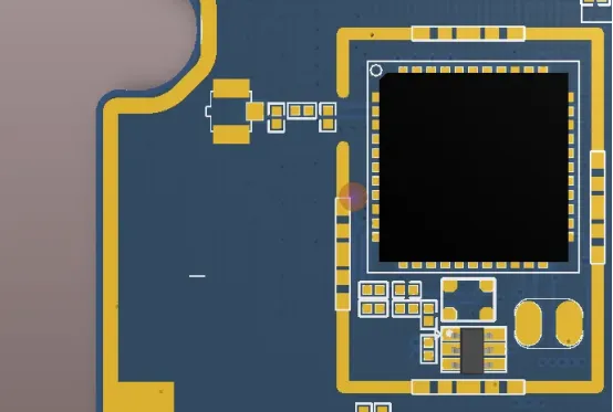
A PCB Shield Can Is Not Just a Metal Lid
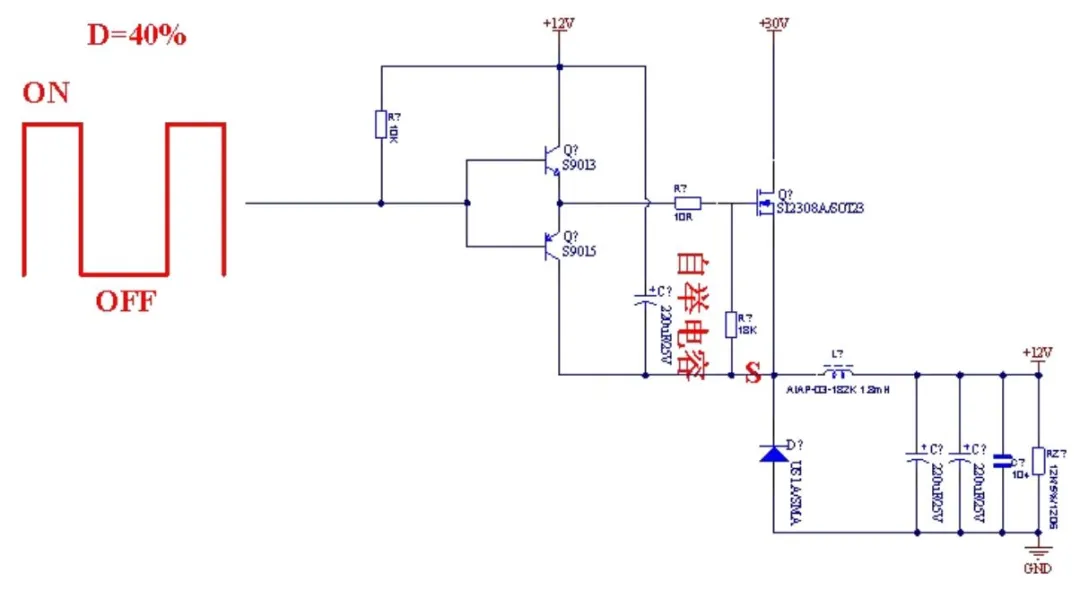
BUCK Converter Hysteretic Circuit: From Principle to Parameter Calculation
Testing SW Signals in DC-DC Converters
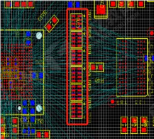
How a Series Resistor on a PCB Improves Signal Integrity
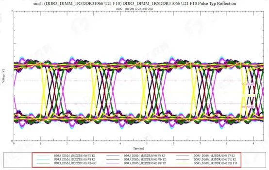
DDR Signal Integrity: Effects of Termination Resistors

5 Practical ESD Design Tips
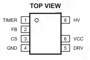
AC-DC Power Conversion: Circuit Methods, HFC0500 Example, and PCB Layout Rules


