Coupons
Help
  • FAQ
    browse most common questions
  • Live Chat
    talk with our online service
  • Email
    contact your dedicated sales:

PCB Manufacturing

Printed Circuit Boards (PCBs) form the backbone of modern electronics, serving as the essential platform where components connect to create functional devices. In the PCB Manufacturing category, readers gain access to a comprehensive collection of resources designed to demystify the intricate processes involved in producing these critical elements. From initial design considerations to final assembly and testing, this category covers every stage, providing valuable insights for engineers, hobbyists, and industry professionals alike. Understanding PCB manufacturing is crucial for anyone involved in electronics development. This field encompasses a wide range of topics, including material selection, such as FR-4 substrates and advanced laminates, as well as fabrication techniques like etching, drilling, and soldering. Articles here delve into best practices for optimizing layouts to minimize signal interference, ensuring reliability in high-stakes applications. Tutorials guide users through prototyping methods, while in-depth analyses explore emerging trends like flexible PCBs and additive manufacturing, which are revolutionizing industries from consumer gadgets to aerospace systems. The practical value of mastering PCB manufacturing extends to real-world scenarios, where efficient production can reduce costs, enhance performance, and accelerate time-to-market. For instance, insights on multilayer board construction help in designing compact devices for IoT applications, and discussions on quality control standards prevent common pitfalls in mass production. By engaging with the diverse guides and expert perspectives in this category, readers can build a solid foundation in PCB technologies, apply proven strategies to their projects, and stay ahead in an ever-evolving field. Whether troubleshooting assembly issues or exploring sustainable manufacturing practices, the knowledge shared here empowers informed decision-making and innovation in electronics.

 
Why HDI PCB Manufacturers Add Dummy Copper
PCB Manufacturing Defects Design For Manufacturing (DFM) PCB Copper Weight HDI PCB Stackup Copper Etching Sequential Build-Up PCB Substrate Warpage PCB Lamination

Why HDI PCB Manufacturers Add Dummy Copper

Learn why HDI PCB manufacturers add dummy copper to achieve uniform plating thickness and control board warpage. This article explains real factory CAM strategies for copper balancing, auxiliary copper placement, and how dummy copper HDI PCB designs prevent defects, improve yield, and maintain tight tolerances during sequential lamination and etching processes.

HDI Laser Drilling Mistakes That Affect Manufacturing Yield
PCB Manufacturing Defects Design For Manufacturing (DFM) High-Temperature PCB HDI Technology Microvia Design Via Reliability Laser Drilling Defects PCB Stackup Design

HDI Laser Drilling Mistakes That Affect Manufacturing Yield

Explore common HDI laser drilling problems that reduce manufacturing yield, including via aperture design, depth control, blind via placement, and exceeding laser capabilities. Learn practical design guidelines to improve microvia reliability, plating quality, and overall HDI production success.

Coverlay Opening vs Solder Mask Opening: What's the Difference?
PCB Materials Design For Manufacturing (DFM) PCB Reliability Solder Mask Application Rigid-Flex Design Solder Mask Expansion Solder Mask Defined Flexible PCB Assembly

Coverlay Opening vs Solder Mask Opening: What's the Difference?

FPC coverlay vs solder mask opening: clear explanation of the essential differences, suitable applications, and common design mistakes in flexible PCB manufacturing. Learn when to use coverlay openings for flex areas versus solder mask on rigid sections to improve reliability, yield, and avoid production issues.

How Do FPC Factories Compensate Coverlay Openings in Practice?
Design For Manufacturing (DFM) PCB Design For Assembly (DFA) Solder Mask Misalignment Solder Mask Application Flex PCB Design Stencil Aperture Flex PCB Materials Polyimide Substrate

How Do FPC Factories Compensate Coverlay Openings in Practice?

Factory CAM view on FPC coverlay opening compensation practices. Learn single-side enlargement rules (0.05-0.15mm), stencil-matched adjustments, and how we handle differences from original design to ensure reliable SMT on flex PCB mask areas.

FR4 Stiffener Inner Shrink Rule for FPC Boards
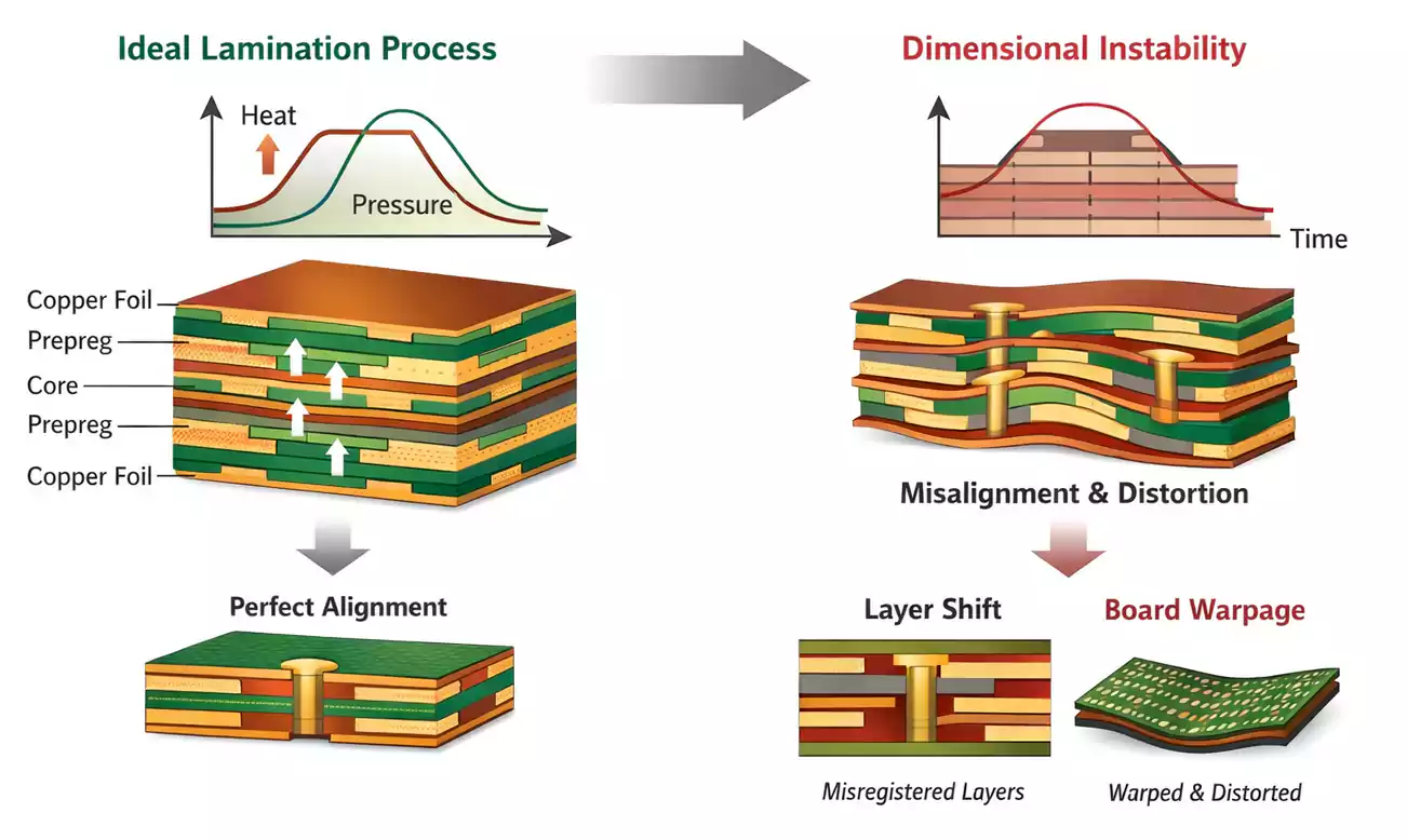
PCB Materials PCB Reliability PCB Warpage Design For Manufacturing Cost Optimization PCB Misalignment Flexible PCB Assembly PCB Lamination

FR4 Stiffener Inner Shrink Rule for FPC Boards

From factory CAM perspective: standard FPC FR4 stiffener shrink rule for outlines and holes (0.15-0.3mm inner offset). Learn real production compensation methods, tolerance matching between lamination vs incoming material, and DFM recommendations to avoid misalignment and yield loss on flex PCB stiffener areas.


2026 AIVON.COM All Rights Reserved
Intellectual Property Rights | Terms of Service | Privacy Policy | Refund Policy