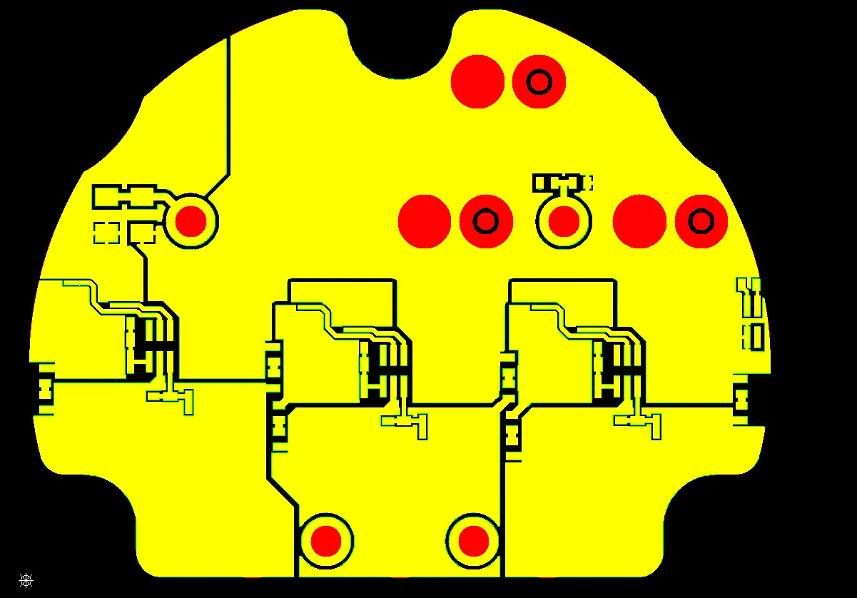
This 4-layer FR-4 board measured 160 mm × 129.5 mm with a finished thickness of 1.6 mm, 1 oz copper on both outer layers, black solder mask, white silkscreen, and ENIG surface finish. The fabrication package specified controlled impedance, a minimum hole size of 0.25 mm, 5 mil line and space, V-cut panelization, and via tenting. During CAM review several interdependent process-capability questions arose, the most significant of which centered on PCB impedance trace width adjustment. The customer notes called for 5 mil single-ended impedance traces, yet stack-up modeling showed that a 7 mil width was required to meet the target impedance on the available dielectric and copper thickness. Additional observations concerning black solder-mask bridges, missing tooling holes, edge-pad clearance, and tented component holes further constrained the manufacturing window.
The engineering assessment focused on whether the requested trace geometry, solder-mask features, and mechanical details could be held repeatably within process tolerances. Each observation was verified against plating, etching, lamination, and routing capability data before any production release.
Single-Ended Impedance Trace Width Adjustment from 5 mil to 7 mil
The processing notes supplied by the customer listed 5 mil impedance lines. When the board ( #FR4-20260312-065 ) stack-up was modeled for a 1.6 mm, 4-layer FR-4 construction with 1 oz outer copper and the dielectric constants typical of KB-6160 TG130 material, the calculated width needed to achieve the intended single-ended impedance was 7 mil. A 5 mil trace on this copper weight and dielectric height would produce a higher impedance than the design target, because the reduced conductor width increases the inductive contribution relative to the capacitive coupling to the reference plane.
Etch factor further narrows the process window. With 1 oz copper the lateral undercut during differential etching typically ranges from 0.3 mil to 0.6 mil per side under controlled conditions. Starting from a 5 mil artwork width therefore risks a finished conductor that is both narrower than intended and more variable from panel to panel. Moving the artwork to 7 mil provides a manufacturing margin that absorbs normal etch variation while still allowing the final plated and etched width to fall inside the impedance tolerance band.
| Parameter | Customer Note | Modeled Requirement | Engineering Assessment |
|---|---|---|---|
| Single-ended trace width | 5 mil | 7 mil | Adjustment required for target Z0 |
| Copper weight | 1 oz | 1 oz | Etch undercut must be compensated |
| Dielectric height (approx.) | Not stated | Consistent with 1.6 mm 4L | Fixed by stack-up |
| Impedance tolerance | Not stated | Typical ±10 % | 5 mil leaves insufficient margin |
A further complication appeared when the impedance-critical nets were marked on the artwork. Certain traces that the customer notes identified as 5 mil impedance lines were later confirmed by the customer as non-impedance nets. Conversely, other conductors that the CAM team had flagged for width adjustment were declared non-critical. Without unambiguous net identification the etching compensation could not be applied selectively. The engineering decision was therefore to adjust the confirmed single-ended PCB impedance traces from 5 mil to 7 mil artwork width, document the change, and obtain formal customer confirmation before panelization.
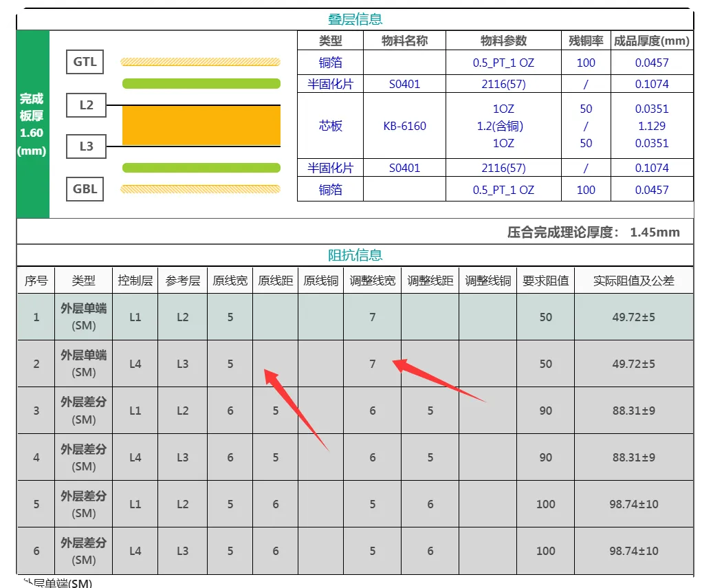
Figure 1: adjust the confirmed single-ended impedance traces from 5 mil to 7 mil artwork width
Black Solder Mask Bridge Limits Below 0.25 mm Component Spacing
Multiple component footprints exhibited pin-to-pin clearances smaller than 0.25 mm. On a black solder-mask finish the minimum reliable solder-mask bridge width is constrained by both registration tolerance and the optical density of the ink. Black formulations typically require a larger minimum bridge than green or other lighter colors because any mis-registration produces a visually unacceptable gap or a residual web that can crack during reflow. Process data for the current black solder-mask system show that bridges narrower than approximately 0.25 mm fall outside the stable process window and frequently result in either incomplete coverage or solder-mask residue on pads.
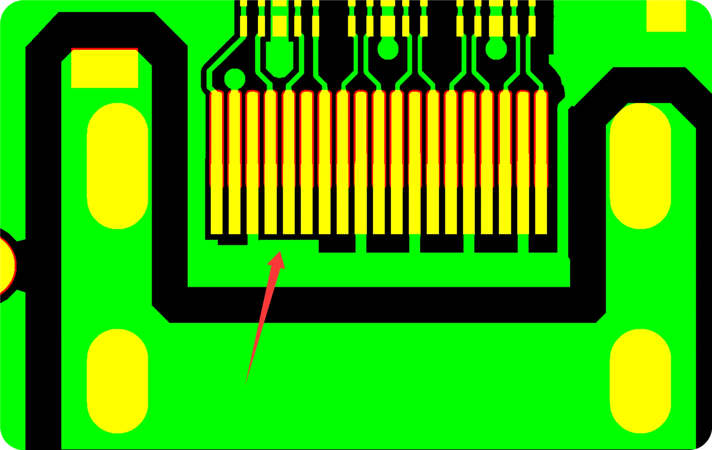

Figure 2,3: multiple component footprints exhibited pin-to-pin clearances smaller than 0.25 mm
The practical resolution was to open the solder-mask windows across these fine-pitch areas rather than attempt to form bridges. Open windows eliminate the risk of mask residue on the pads and maintain the required electrical isolation between adjacent pins. The change was documented and submitted for customer confirmation, because the absence of bridges alters the visual appearance and the solder-mask defined land geometry.
Missing Tooling Holes on Process Edges for Mechanical Routing
The panel design contained no locating holes on the breakaway rails. Mechanical routing of a 1.6 mm FR-4 panel requires fixed reference points to maintain dimensional accuracy and to prevent panel movement under the router bit. Without tooling holes the panel cannot be securely clamped; the resulting positional error can shift the final outline relative to the copper features by several tenths of a millimeter. Four 2.0 mm tooling holes were therefore added on the process edge at locations that do not interfere with the circuit or the V-cut lines. The addition restores a controllable registration datum for the routing operation.
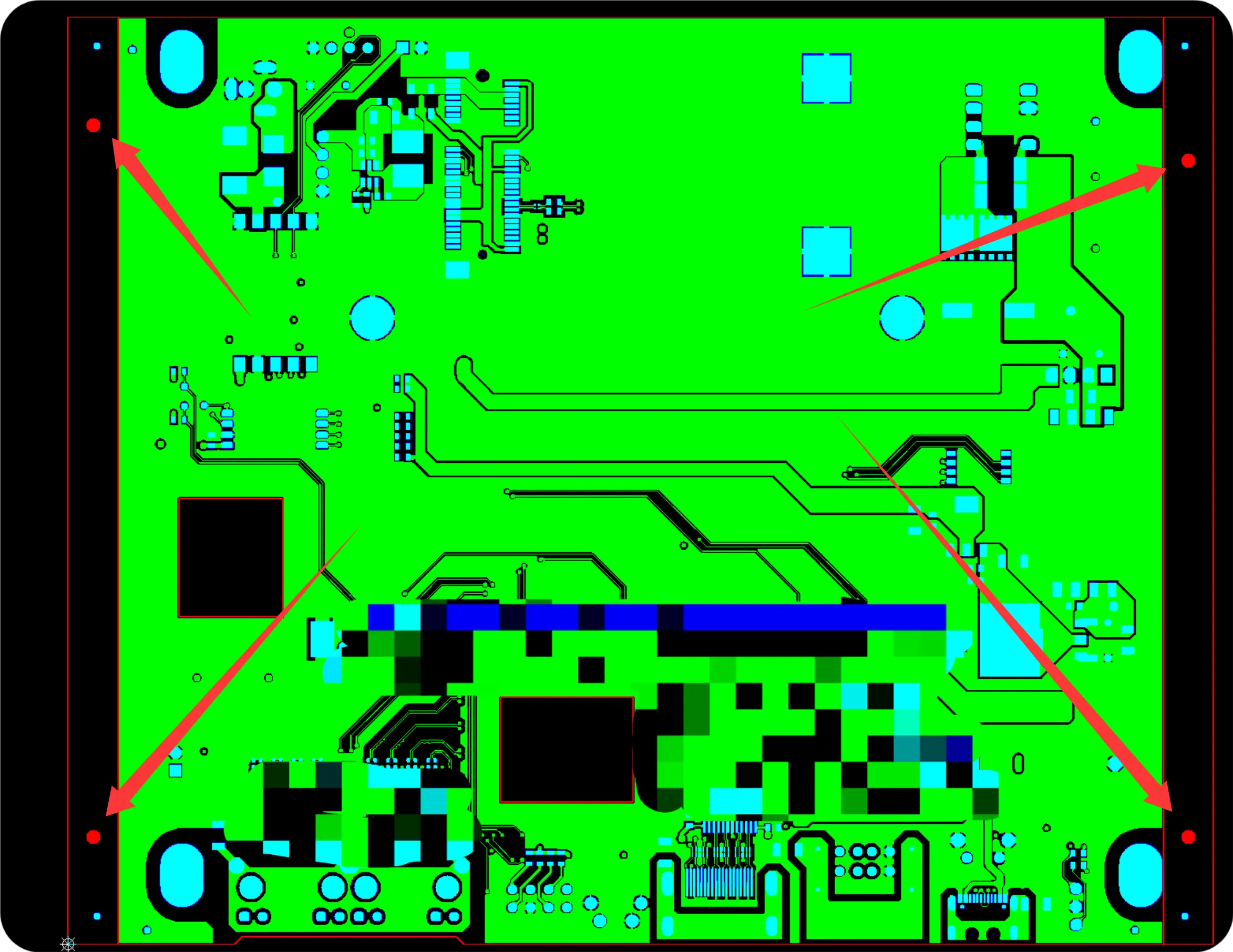
Figure 4: four 2.0 mm tooling holes were therefore added on the process edge
SMD Pad Clearance to Board Edge and Copper Exposure Risk
Several surface-mount pads were positioned close enough to the finished outline that the subsequent mechanical routing step would expose copper at the board edge. Exposed copper on an ENIG-finished board creates both a cosmetic defect and a potential corrosion site. IPC-A-600 classifies such edge exposure as a workmanship issue once the copper extends beyond the solder-mask or the intended land boundary. The engineering recommendation was to trim the affected pads so that a minimum copper-to-edge clearance is retained after routing. Confirmation was requested because pad trimming reduces the available solderable area and must be accepted by the designer.
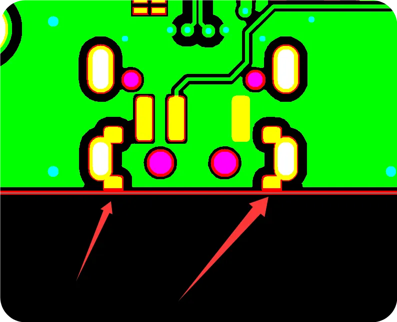
Figure 5: several pads were positioned close enough to the finished outline
Solder Mask Tenting over Component Holes and Resulting Diameter Reduction
A subset of component holes had been designed with full tenting. When black solder mask is applied over these holes the liquid ink flows into the plated barrels. After curing the residual ink reduces the effective hole diameter and leaves a non-wettable surface that prevents reliable soldering. Process experience with 0.25 mm and larger holes shows that even a thin tenting film can shrink the finished diameter below the insertion or soldering tolerance. The correct treatment for component holes is therefore an open solder-mask aperture. The CAM data were revised to open the mask over these holes while retaining tenting only on the non-component vias, preserving the original electrical isolation intent without compromising solderability.
Physical Process Windows for Etching, Masking and Mechanical Forming
Controlled-impedance etching on 1 oz copper operates inside a relatively narrow window once line widths approach 5 mil. The combination of etch undercut, copper thickness variation, and dielectric height tolerance must remain inside the impedance budget. Increasing the artwork width to 7 mil restores a usable margin without requiring a change in copper weight or stack-up. Black solder-mask registration and cure add a second constraint: the optical density of the ink amplifies any misalignment, making sub-0.25 mm bridges statistically unreliable. Mechanical routing without tooling holes further narrows the dimensional window for the finished outline.
The integrated process sequence that satisfied all constraints was:
- Impedance modeling confirming 7 mil artwork for single-ended nets
- Selective width adjustment and customer confirmation of net identity
- Solder-mask data revised to open windows on sub-0.25 mm pitch and on component holes
- Addition of 2.0 mm tooling holes on process edges
- Pad trimming at outline-critical locations
- Standard ENIG, V-cut, and electrical test
Each step was verified against existing process-capability indices for etching uniformity, solder-mask registration, and mechanical dimensional control before the revised data package was released.
| Process Element | Original Condition | Adjusted Condition | Capability Margin |
|---|---|---|---|
| Impedance trace width | 5 mil artwork | 7 mil artwork | Restored |
| Solder-mask bridges | <0.25 mm | Open windows | Stable |
| Tooling holes | Absent | 2.0 mm added | Routing datum restored |
| Edge-pad clearance | Insufficient | Pads trimmed | Copper exposure eliminated |
| Component-hole tenting | Full tent | Open apertures | Solderability preserved |
Capability Verification by Cross-Section and Electrical Test
Prototype panels incorporating the 7 mil impedance traces, open solder-mask windows, added tooling holes, trimmed edge pads, and open component-hole apertures were processed through the standard sequence. Cross-section measurements confirmed that the finished conductor widths after etch and plating fell within the impedance tolerance band. Solder-mask registration on the black finish showed clean openings without residual webs on the fine-pitch pads. Dimensional inspection verified that the tooling holes provided stable registration for mechanical routing and that the trimmed pads retained adequate copper-to-edge clearance. Flying-probe continuity and impedance sampling on the adjusted nets met the acceptance criteria. These results established that the revised data package operated inside a repeatable manufacturing window.
Approved Manufacturing Window and Release Decision
The final disposition retained the original 4-layer stack-up, 1 oz copper, black solder mask, and ENIG finish while implementing five controlled adjustments: (1) single-ended impedance artwork widened from 5 mil to 7 mil, (2) solder-mask bridges replaced by open windows on sub-0.25 mm pitch, (3) 2.0 mm tooling holes added on process edges, (4) edge-critical SMD pads trimmed, and (5) component holes opened through the solder mask. These changes restored usable process margins for etching uniformity, mask registration, mechanical registration, and solderability without altering the functional copper pattern or the target impedance value.
The case demonstrates that PCB impedance trace width adjustment is not merely a numerical change; it defines the boundary between a design that can be etched and plated to a stable impedance and one that will exhibit excessive variation once normal process tolerances are applied. By quantifying the capability margins for trace width, solder-mask bridges, tooling, edge clearance, and tenting, the engineering team converted an otherwise marginal data package into a production-ready construction.
FAQ
Q1: Why is a 5 mil single-ended impedance trace often adjusted to a wider artwork width on 1 oz copper?
A1: Etch undercut on 1 oz copper removes 0.3–0.6 mil per side. A 5 mil artwork therefore finishes narrower than the impedance model requires, shifting the characteristic impedance upward. Increasing the artwork to 7 mil compensates for the undercut and restores the finished width needed for the target impedance on a typical 1.6 mm 4-layer stack-up.
Q2: Why can black solder mask not reliably form bridges below 0.25 mm pin spacing?
A2: Black ink has higher optical density and greater registration sensitivity. Bridges narrower than approximately 0.25 mm fall outside the stable process window, producing either incomplete coverage or residual webs that crack during reflow. Opening the solder-mask windows eliminates both defects while preserving electrical isolation.
Q3: What is the consequence of missing tooling holes on the process edge of a mechanically routed panel?
A3: Without fixed locating holes the panel cannot be securely clamped under the router. Positional drift of several tenths of a millimeter relative to the copper features becomes probable. Adding 2.0 mm tooling holes on the breakaway rails restores a controllable registration datum and keeps the finished outline within tolerance.
Q4: Why must SMD pads near the board edge sometimes be trimmed?
A4: Mechanical routing removes material at the outline. Pads that extend too close to the edge leave exposed copper after forming. Exposed copper is both a cosmetic and a corrosion concern under IPC-A-600. Trimming the pads restores a minimum copper-to-edge clearance while retaining sufficient solderable area.
Q5: Why is full solder-mask tenting unsuitable for component holes?
A5: Liquid solder mask flows into the plated barrels and remains after cure, reducing the finished hole diameter and creating a non-wettable surface. Component holes therefore require open apertures so that soldering can occur without diameter loss or contamination.
Q6: How does unambiguous net identification affect impedance trace width adjustment?
A6: Selective width compensation can be applied only to the nets that are truly impedance-controlled. When customer notes and artwork markings conflict, the manufacturer cannot determine which traces require the adjusted width. Formal confirmation of net identity is therefore a prerequisite for any impedance-related artwork change.
```