During CAM review of a 4-layer FR-4 TG150 board measuring 427.5 mm × 316.4 mm with 1.6 mm finished thickness, mixed 1 oz inner / 2 oz outer copper, and lead-free HASL surface finish, several process capability questions were raised. The customer required IPC Class 3 acceptance criteria and explicitly noted that the panel incorporates a chamfer. Combined with a request for precision routing of the outline, missing stamp holes at bridge locations, and incomplete solder-mask openings in the gold-finger region, these elements triggered a formal engineering evaluation to determine whether the design could be manufactured with consistent edge quality and mechanical reliability.
Project Requirements and Technical Challenges in Precision Outline Routing
The order ( #FR4-20260507-071 )specified a 4-layer construction using FR-4 TG150 material, board thickness 1.6 mm, outer copper 2 oz and inner copper 1 oz, minimum hole diameter 0.3 mm, and line width/space of 6 mil. Panelization was customer-supplied (2-up), with V-scoring plus milling, no process border, and mechanical forming. Delivery target was 13 days. Customer remarks stated "IPC – CLASS 3 IS NECESSARY PANEL IT HAS A CHAMFER."
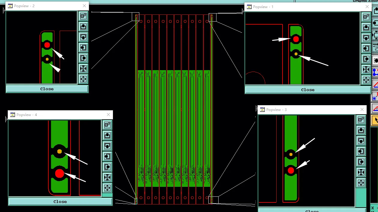
The core technical challenges centered on three interrelated process items. First, the customer requested confirmation that the outline would be produced by precision routing rather than standard milling. Second, the supplied Gerber data contained no stamp holes at the bridge (tab) locations that connect individual boards within the panel. Third, the gold-finger areas lacked designed solder-mask openings, which would leave residual solder mask on surfaces intended for edge-contact reliability under Class 3 criteria. In parallel, our standard 4-layer TG150 stackup was submitted for customer confirmation.
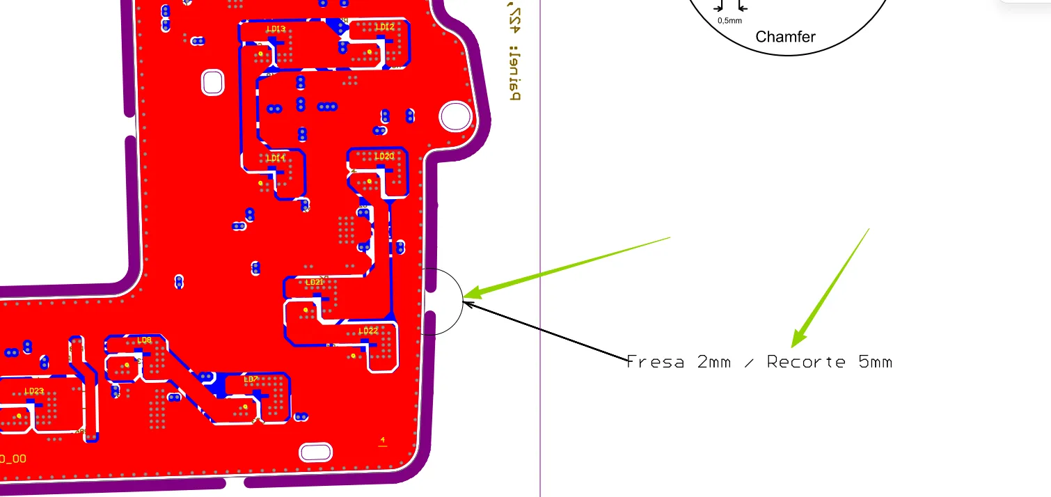
Figure 1: there's no stamp holes in the arrow part
| Manufacturing Parameter | Order Requirement | Typical Process Capability | Engineering Assessment |
|---|---|---|---|
| Outline Process | Precision routing | Standard CNC milling | Required for chamfer edge quality |
| Acceptance Class | IPC Class 3 | Class 2 standard | Elevates edge and plating criteria |
| Stamp Holes at Bridges | Not designed | Recommended for customer panel | Must be added for controlled break |
| Gold-Finger Mask Openings | Missing in original data | Full clearance required | Risk of residual mask on contact surface |
Why Precision Routing Became the Primary Capability Question
Our process review noted that the panel incorporates a chamfer and must meet IPC Class 3 visual and dimensional criteria. Standard milling leaves a characteristic tool-mark texture and a larger radius at internal corners. Precision routing employs a finer tool path strategy, reduced step-over, and tighter positional control to produce smoother edges and sharper chamfer transitions. Without this process change, the risk of Class 3 rejection for edge roughness or incomplete chamfer geometry would increase.
Physical Limits of Outline Routing and Panel Depaneling
CNC routing of FR-4 is governed by spindle rigidity, tool deflection, and heat generation in the glass-resin matrix. When a chamfer is required, the tool must follow a multi-pass path that simultaneously controls depth of cut and lateral position. Under IPC-A-600 Class 3 standard, edge defects such as chipping, delamination, or excessive roughness are more strictly limited than under Class 2. Precision routing narrows the process window but improves edge integrity when the machine parameters and tooling are correctly matched to the 1.6 mm TG150 laminate.
Stamp holes (also called mouse bites) serve as controlled fracture points at the bridges. Their absence in the original data meant that any attempt to separate the boards would rely solely on V-score residual thickness or uncontrolled manual break, both of which raise the probability of edge damage on a Class 3 panel. Adding properly sized and spaced stamp holes restores a predictable break force and protects the chamfered edges.
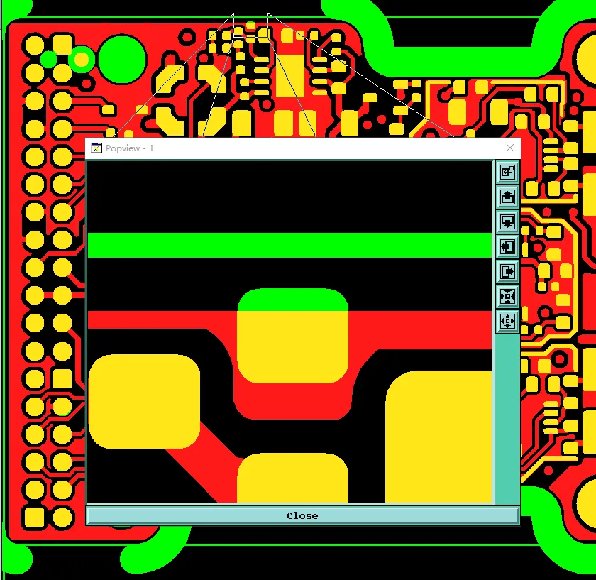
For the gold-finger region, residual solder mask left by an unopened window would interfere with subsequent contact reliability. Although the specified surface finish is lead-free HASL, the design intent for gold-finger geometry still requires complete mask clearance so that the plated surface is fully accessible and free of organic residue.
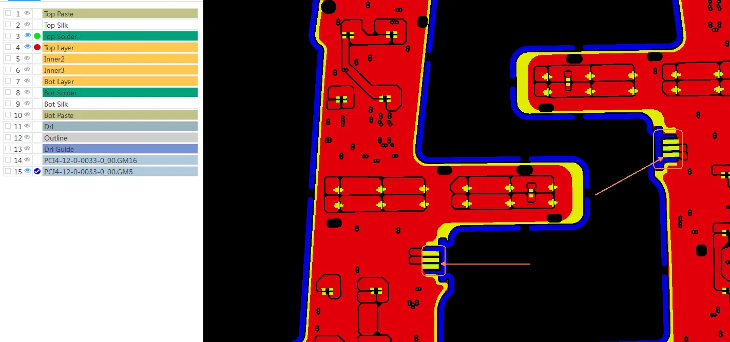
Figure 2: it didn't fully open mask for the golden finger
| Process Variable | Standard Milling | Precision Routing | Impact on Class 3 Yield |
|---|---|---|---|
| Edge roughness | Higher tool marks | Reduced surface texture | Improved visual acceptance |
| Chamfer geometry | Larger corner radius | Tighter dimensional control | Meets chamfer tolerance more consistently |
| Tool deflection risk | Moderate | Lower with optimized feeds | Better registration to copper features |
Engineering Evaluation of Stackup and Panelization Controls
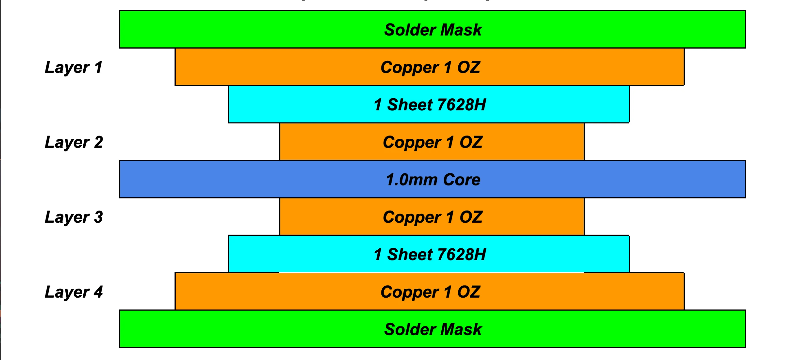
Our internal 4-layer TG150 stackup for 1.6 mm finished thickness with 1 oz / 2 oz copper distribution was verified against the customer data. Copper balance remained within acceptable limits for warpage control, and the dielectric thicknesses supported the required mechanical strength for a chamfered panel. Customer confirmation of the stackup was requested as a formal step before release.
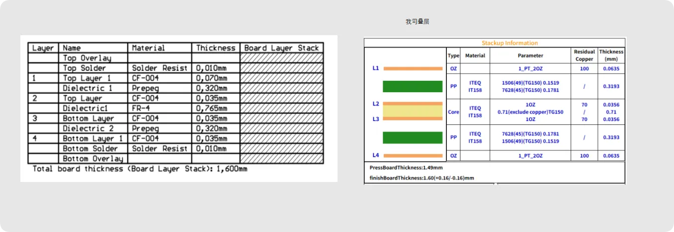
Figure 3: the stack up we offered
For the missing stamp holes, the engineering recommendation was to add them at the bridge locations using a standard diameter and pitch that provide sufficient residual strength during handling yet allow clean separation. This modification was presented as a process-necessary addition rather than a design change, ensuring the customer panel could be depanelled without compromising the precision-routed edges or the chamfer.
The gold-finger solder-mask openings were treated similarly: the absence of openings in the original data was flagged, and confirmation was requested to open the windows fully. Leaving mask over the contact area would create an immediate Class 3 defect risk under IPC-A-600 visual criteria for surface cleanliness and plating exposure.
Capability Assessment of Precision Routing Equipment
Our CNC routing platforms are equipped with high-speed spindles and closed-loop positioning that support the reduced step-over and multi-pass strategies required for precision outline work. Tool selection, feed rate, and spindle speed were evaluated against the 1.6 mm TG150 material to keep cutting forces low enough to avoid edge chipping while still achieving the dimensional accuracy demanded by the chamfer. The process window remains stable provided the tooling is replaced at the prescribed interval and vacuum fixturing holds the panel flat.
| Control Item | Action Taken | Process Margin |
|---|---|---|
| Outline method | Confirmed precision routing | Adequate for Class 3 edge quality |
| Stamp-hole addition | Recommended and positioned at bridges | Restores controlled depaneling |
| Gold-finger mask windows | Requested full opening | Eliminates residual-mask risk |
| Stackup verification | Standard 4-layer TG150 confirmed | Within thickness and balance limits |
Validation Through Prototype Routing and Inspection
Prototype panels were processed with the confirmed precision-routing parameters. Edge roughness was measured and compared against Class 3 limits; results remained comfortably inside the acceptance window. Chamfer geometry was verified by optical measurement at multiple points along the panel perimeter. Stamp holes were added and subjected to controlled break tests to confirm that the residual web strength was sufficient for handling yet low enough for clean separation without edge fracture.
Cross-section samples taken near the routed edges showed no delamination or copper lifting attributable to the routing process. Solder-mask openings in the gold-finger zones were inspected under magnification to ensure complete clearance and clean edges. All measurements supported release of the adjusted data package for production.
Conclusion
The combination of precision routing, addition of stamp holes at the bridge locations, full solder-mask openings over the gold-finger areas, and confirmation of the standard 4-layer TG150 stackup brought the design inside a stable manufacturing process window. These adjustments addressed the specific capability concerns raised by the IPC Class 3 requirement and the presence of a chamfer on the panel. With the engineering questions resolved and the process parameters locked, the order proceeded to production under controlled conditions that maintain both edge quality and mechanical integrity.
This case illustrates how targeted process confirmation and minor, well-documented data adjustments allow a customer panel with elevated acceptance criteria to be manufactured reliably without expanding the overall process capability envelope beyond proven limits.
FAQ
Q1: Why is precision routing preferred over standard milling when a panel has a chamfer and must meet IPC Class 3?
A1: Precision routing uses finer tool paths and reduced step-over to produce smoother edges and more accurate chamfer geometry. Standard milling leaves more pronounced tool marks and larger corner radii that can fall outside Class 3 visual and dimensional limits.
Q2: What manufacturing risk exists if stamp holes are omitted from customer-panel bridges?
A2: Without stamp holes the boards must be separated by V-score residual thickness alone or by uncontrolled force. Either approach increases the chance of edge chipping or fracture that would violate Class 3 acceptance criteria, especially on a chamfered contour.
Q3: Can a standard 4-layer TG150 stackup support mixed 1 oz / 2 oz copper while remaining within thickness tolerance?
A3: Yes. The dielectric thicknesses and copper distribution of a typical 1.6 mm 4-layer TG150 construction accommodate the copper weights with sufficient process margin for both thickness uniformity and warpage control under normal lamination conditions.
Q4: Why must solder-mask openings be present over gold-finger areas even when the surface finish is lead-free HASL?
A4: Residual solder mask on the contact surface creates an immediate visual and functional defect under IPC Class 3. Full openings ensure the plated metal is clean and accessible regardless of the specific surface-finish chemistry.
Q5: How does tool deflection affect edge quality on a 1.6 mm FR-4 panel?
A5: Excessive deflection produces positional error and can leave uneven or chipped edges. Precision-routing parameters keep cutting forces low enough that deflection remains inside the tolerance required for chamfer accuracy and Class 3 edge appearance.
Q6: What is the practical benefit of confirming the manufacturer’s standard stackup before production release?
A6: Confirmation aligns the design with proven material inventory and press parameters, eliminating uncertainty about dielectric thickness, copper balance, and final board thickness. This step shortens the path to a stable, repeatable process window.