










PCB Design
Printed Circuit Board (PCB) design forms the backbone of modern electronics, enabling the creation of compact, efficient, and reliable devices that power everything from smartphones to industrial machinery. In this category, readers gain access to a comprehensive collection of resources dedicated to mastering PCB design principles and techniques. Whether you are a seasoned engineer refining complex layouts or a newcomer learning the fundamentals, these articles provide the knowledge needed to tackle real-world challenges in electronics development. The scope of PCB design covered here extends from initial schematic capture to final board fabrication and testing. Articles delve into essential topics such as layer stacking, signal integrity, thermal management, and component placement strategies. Guides and tutorials offer step-by-step instructions for using popular software tools like Altium Designer and KiCad, while insights explore emerging trends like flexible PCBs and high-speed designs. Best practices emphasize error reduction, cost optimization, and compliance with industry standards, ensuring designs are not only functional but also manufacturable at scale. Real-world applications highlight the category's practical value, demonstrating how effective PCB design contributes to innovations in automotive systems, medical equipment, renewable energy solutions, and consumer gadgets. By addressing common pitfalls and sharing expert tips, these pieces equip professionals to enhance product performance and reliability. Readers benefit from building a deeper understanding through interconnected articles that cover foundational concepts alongside advanced methodologies, fostering continuous improvement in electronics projects. For those involved in prototyping or production, the technical relevance of this content lies in its focus on efficiency and innovation. Detailed discussions on impedance control, EMI shielding, and design for manufacturability prepare you to meet the demands of today's fast-paced tech landscape. Engaging with multiple articles in this category allows for a progressive learning path, where foundational knowledge supports exploration of specialized topics, ultimately leading to more robust and innovative PCB designs.
Latest Blogs
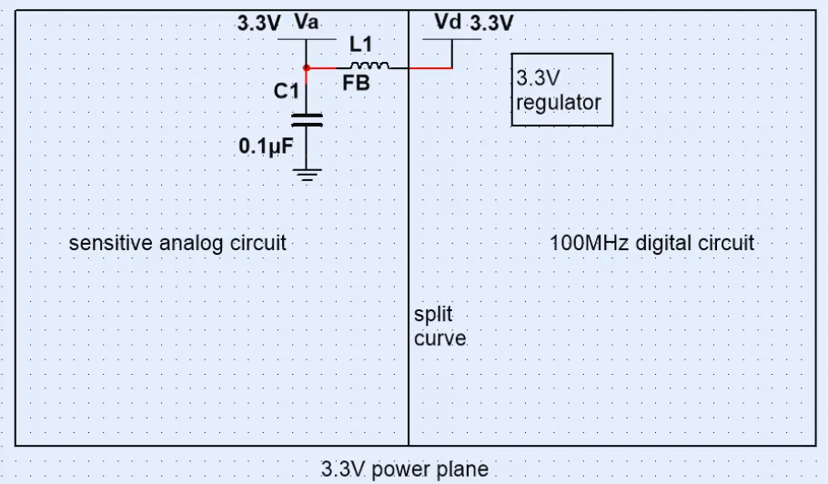
When and Why to Split Power Planes in PCB Design
Explore the reasons for splitting power planes in PCB design, including advantages, disadvantages, and best practices for isolating power domains in mixed-signal boards.
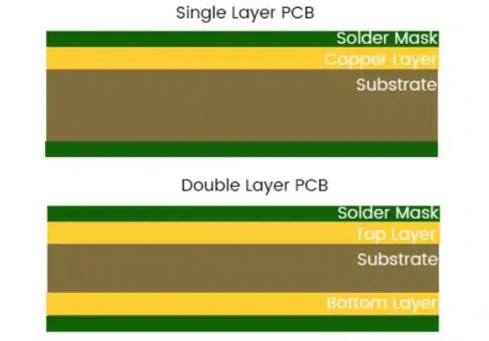
Understanding PCB Basics: Layers, Traces, and Vias Explained
Learn PCB basics with our guide on layers, traces, and vias. Perfect for hobbyists exploring single vs double layer PCB design and terminology.
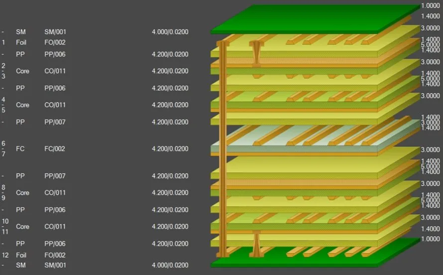
Understanding The PCB Stackup
Explore the essentials of PCB stackup design for electrical engineers. Learn best practices for signal integrity and optimal performance in multilayer PCBs.
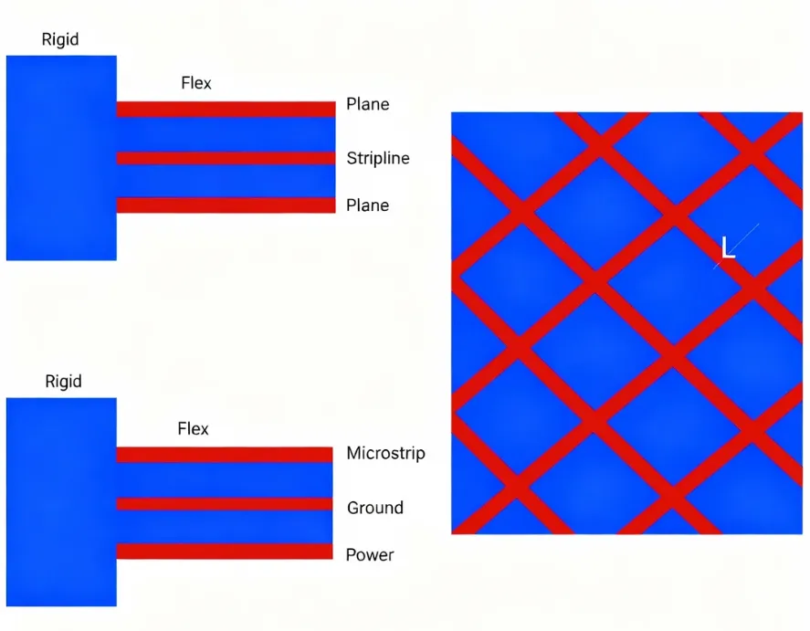
Solid vs. Hatched Power Planes: Which Should You Choose for Your PCB Design?
Explore the differences between solid and hatched power planes in PCB design, their impact on performance, cost, and manufacturing, and how to choose the right one for your project.
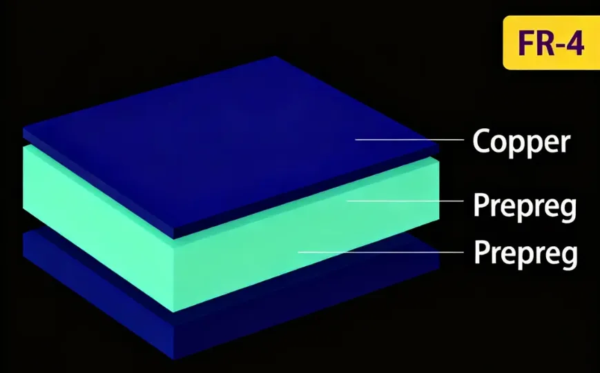
PCB Prepreg Thickness: A Designer's Guide to Stackup, Materials, and Performance
Understand the critical role of prepreg thickness in PCB design, covering material selection, stackup strategies, impedance control, and overcoming manufacturing challenges.
Designing Wearable PCBs with KiCad: A Step-by-Step Guide
Learn to design compact and efficient printed circuit boards for wearable electronics using KiCad, the powerful open-source PCB design software.
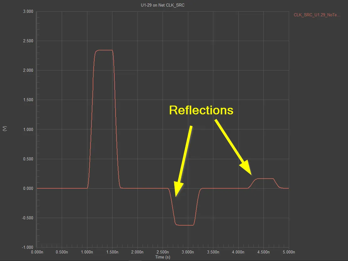
How to Reduce Signal Reflection on PCBs with Proper Impedance Design
Minimize signal reflection in high-speed PCB designs. This guide details controlled impedance, continuous planes, and proper termination for optimal signal integrity and reduced bit errors.
6-Layer PCB Design for High-Frequency Amplifiers: Optimizing Performance and Stability
Master 6-layer PCB RF amplifier design with expert tips on impedance matching, RF grounding, isolation techniques, and stability analysis. Optimize high-frequency performance for wireless and radar apps. AIVON shares practical assembly insights for reliable builds.
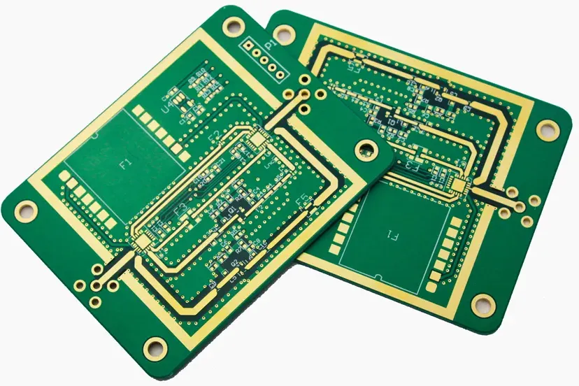
ENIG Surface Finish for High-Frequency PCBs: Impact on Signal Integrity
ENIG surface finish delivers flat, reliable plating for high-frequency PCBs, but the nickel layer and 2 microinches gold thickness can increase insertion loss above 5 GHz. Explore its impact on signal integrity, impedance control, and proven mitigation strategies for RF and 5G designs. Get expert PCB manufacturing insights today.
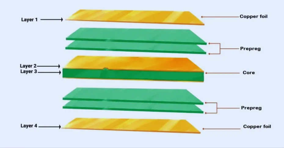
Designing a 4-Layer PCB Stackup: Enhancing Signal Integrity and Performance
Explore how to design an effective 4-layer PCB stackup for optimal signal integrity, noise reduction, and performance in modern electronic applications.
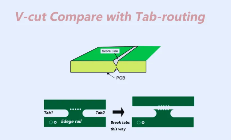
PCB Panelization: V-Cut vs. Tab-Routing for Efficient Manufacturing
Compare V-cut vs tab routing for PCB panelization to maximize manufacturing efficiency, reduce waste, and minimize stress. This guide covers design rules, cost analysis, hybrid approaches, mouse bites, and DFM best practices for higher yield in prototype and production runs.
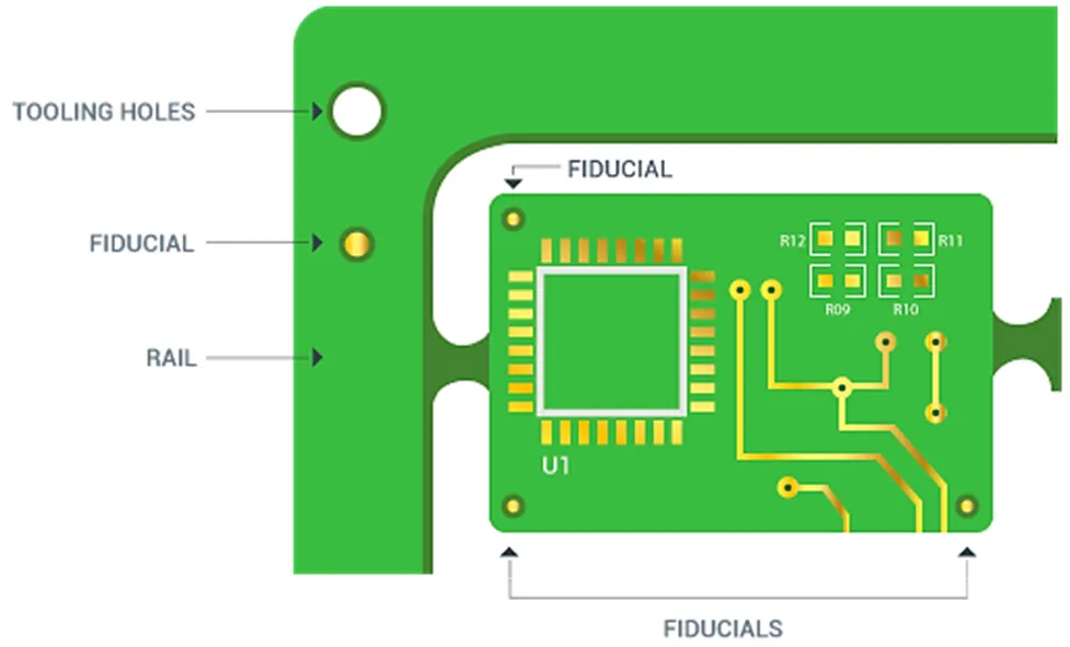
PCB Mounting Holes and Outlines: A Comprehensive Design Guide
What is the mounting holes meaning in electronics? This guide explores everything about mounting holes PCB design, including how to choose the correct PCB mounting hole size for M3 screws, PTH vs. NPTH types, and placement strategies for EMI shielding.


