


PCB Design
Printed Circuit Board (PCB) design forms the backbone of modern electronics, enabling the creation of compact, efficient, and reliable devices that power everything from smartphones to industrial machinery. In this category, readers gain access to a comprehensive collection of resources dedicated to mastering PCB design principles and techniques. Whether you are a seasoned engineer refining complex layouts or a newcomer learning the fundamentals, these articles provide the knowledge needed to tackle real-world challenges in electronics development. The scope of PCB design covered here extends from initial schematic capture to final board fabrication and testing. Articles delve into essential topics such as layer stacking, signal integrity, thermal management, and component placement strategies. Guides and tutorials offer step-by-step instructions for using popular software tools like Altium Designer and KiCad, while insights explore emerging trends like flexible PCBs and high-speed designs. Best practices emphasize error reduction, cost optimization, and compliance with industry standards, ensuring designs are not only functional but also manufacturable at scale. Real-world applications highlight the category's practical value, demonstrating how effective PCB design contributes to innovations in automotive systems, medical equipment, renewable energy solutions, and consumer gadgets. By addressing common pitfalls and sharing expert tips, these pieces equip professionals to enhance product performance and reliability. Readers benefit from building a deeper understanding through interconnected articles that cover foundational concepts alongside advanced methodologies, fostering continuous improvement in electronics projects. For those involved in prototyping or production, the technical relevance of this content lies in its focus on efficiency and innovation. Detailed discussions on impedance control, EMI shielding, and design for manufacturability prepare you to meet the demands of today's fast-paced tech landscape. Engaging with multiple articles in this category allows for a progressive learning path, where foundational knowledge supports exploration of specialized topics, ultimately leading to more robust and innovative PCB designs.
Featured Blog
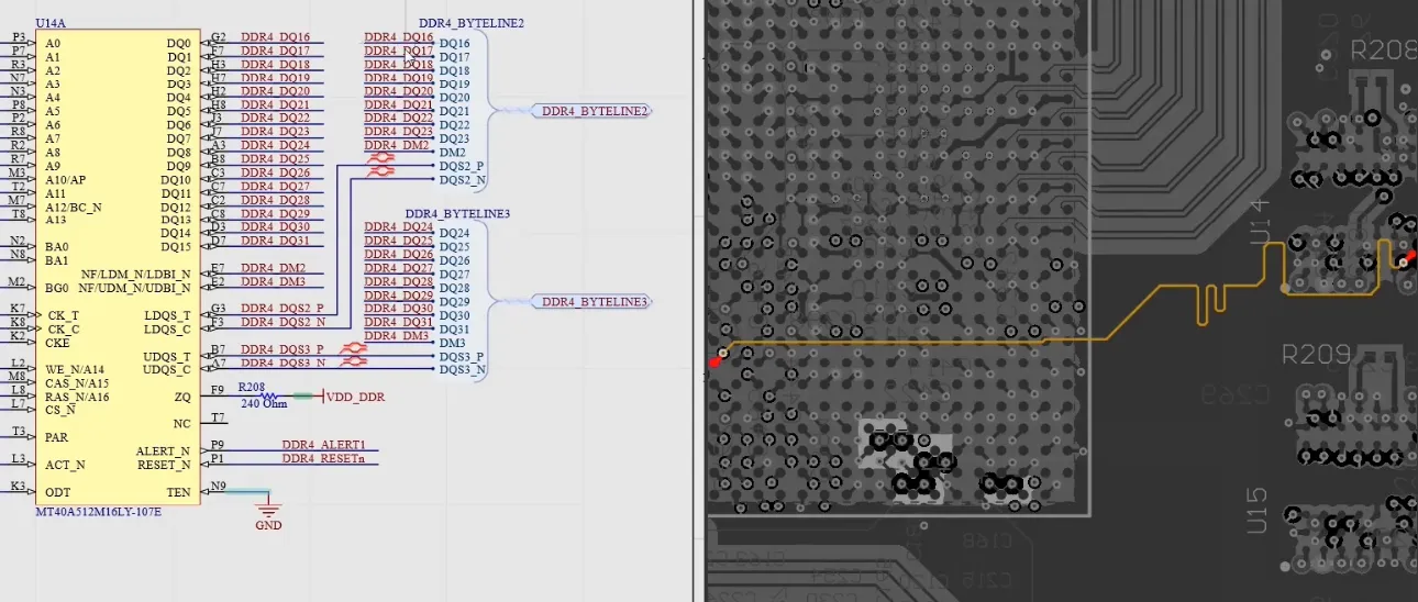
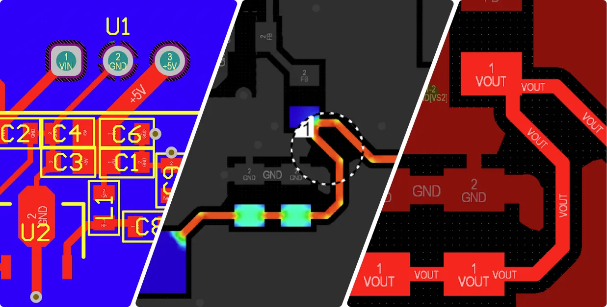
PCB Design Review for Beginners: A Step by Step Guide
Learn how to perform a PCB design review with a practical checklist covering schematics, layout, DRC, manufacturability, and pre-production checks.
Latest Blogs
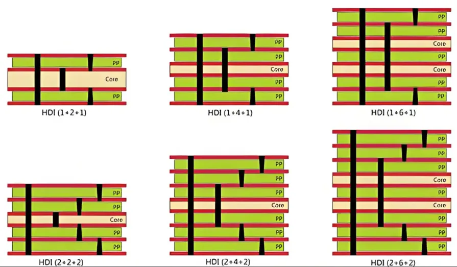
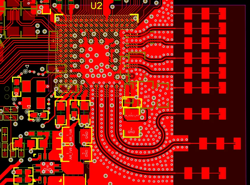
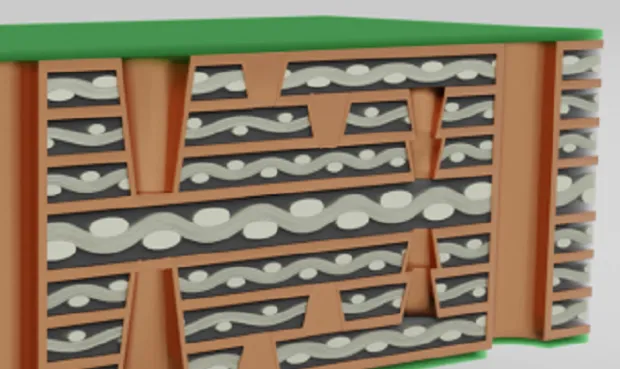
HDI PCB Microvia: A Comprehensive Guide to Design, Reliability, and Manufacturing
Master microvia design for HDI PCB applications, including microvia size, microvia-in-pad, laser drilling, stacked structures, reliability, and impedance control. Explore practical microvia PCB design strategies for high-density routing and reliable HDI manufacturing.
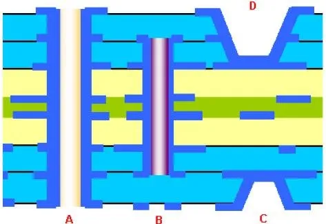
High Reliability Blind Via Design: Meeting Stringent Industry Standards
Implement high reliability blind via in aerospace PCB design, medical PCB design, and automotive PCB design with IPC standards blind via guidelines. Explore technical principles, challenges, best practices, and troubleshooting for robust performance in extreme conditions. Ensure failure-free interconnects.
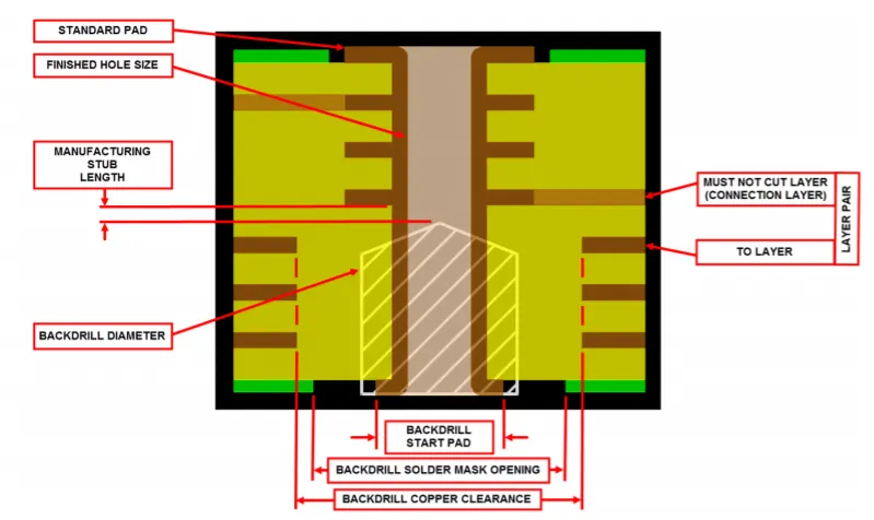
Backdrilling and Blind Vias: A Combined Approach to Signal Integrity
Backdrilling blind vias reduce via stubs to improve signal integrity in high speed PCB designs. This guide details technical principles, controlled impedance strategies, best practices, and IPC standards for engineers tackling multilayer challenges and reflections.
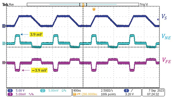
Crosstalk in High Speed Digital Design: Challenges and Solutions
High speed digital design crosstalk causes signal noise from trace coupling. Mitigate challenges with strategies like 3W spacing, guard traces, reference planes, and stackups to ensure signal integrity high speed design in PCBs.
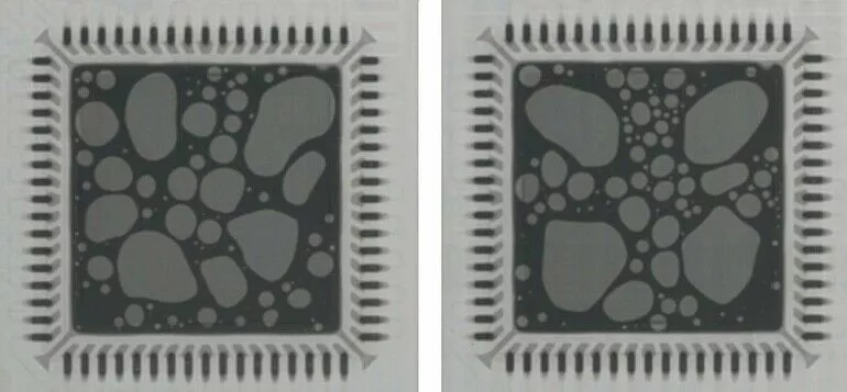
QFN Package Soldering: Thermal Pad Design and Void Reduction
Learn about QFN packages, exposed thermal pad design, and QFN package soldering. Explore PCB footprint layout, solder paste control, stencil patterns, and reflow techniques to reduce voids and improve SMT assembly reliability.
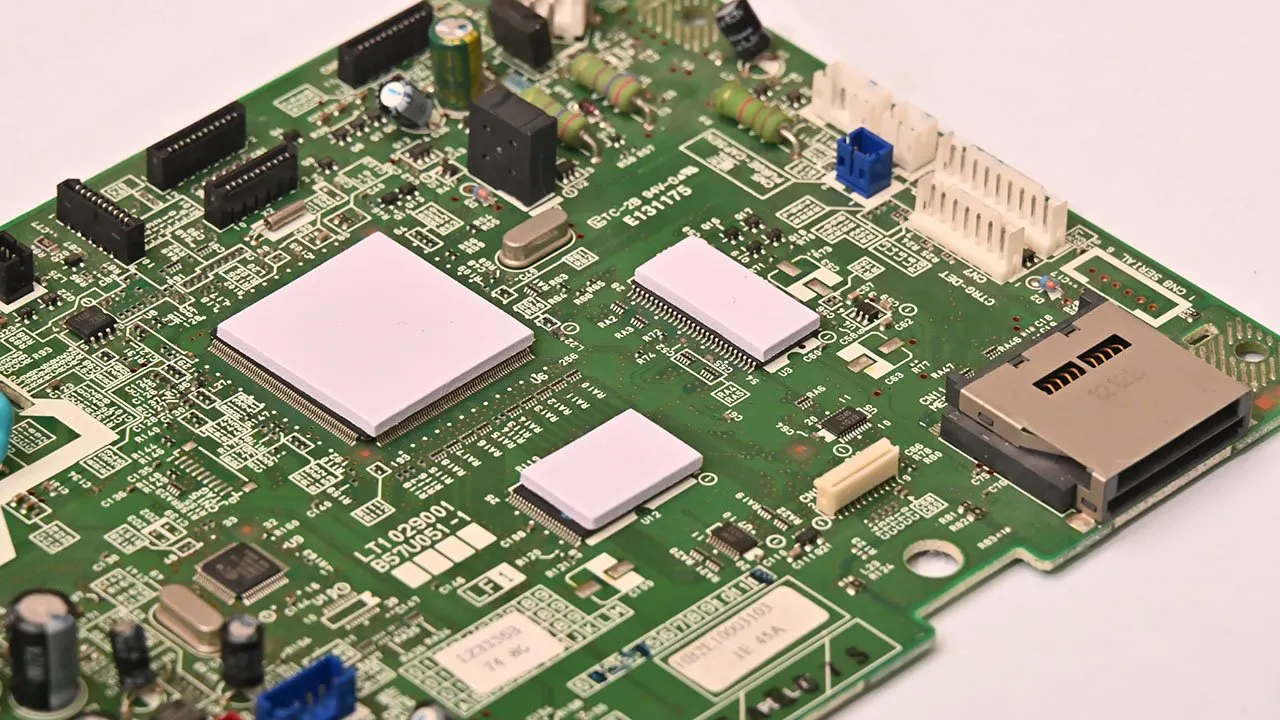
The Ultimate Guide to Thermal Pad Materials: Choosing the Right One for Your Electronic Project
Covering thermal pad material conductivity, silicone vs non-silicone thermal pads, graphite thermal pad properties, durometer, and breakdown voltage. Electric engineers gain practical criteria to select reliable thermal pads for high-performance electronic projects.
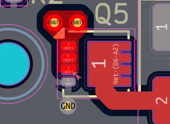
Optimizing Thermal Pad Design for High Power PCB Components: A Comprehensive Guide
Master PCB thermal pad design for high-power components like MOSFETs. Learn size optimization, thickness, strategic thermal via placement, and high current PCB thermal design best practices to prevent hotspots and boost reliability.
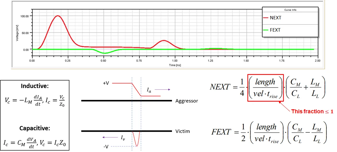
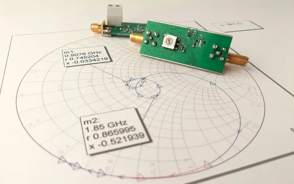
The Impact of Impedance Control on Crosstalk: A Comprehensive Analysis
Impedance mismatches trigger reflections that amplify crosstalk in high-speed PCBs. Impedance control maintains consistent trace Z0 to curb noise coupling between lines. This analysis covers mechanisms of impedance control crosstalk, best practices for controlled impedance PCBs, quantitative insights, and IPC standards for verification and design.
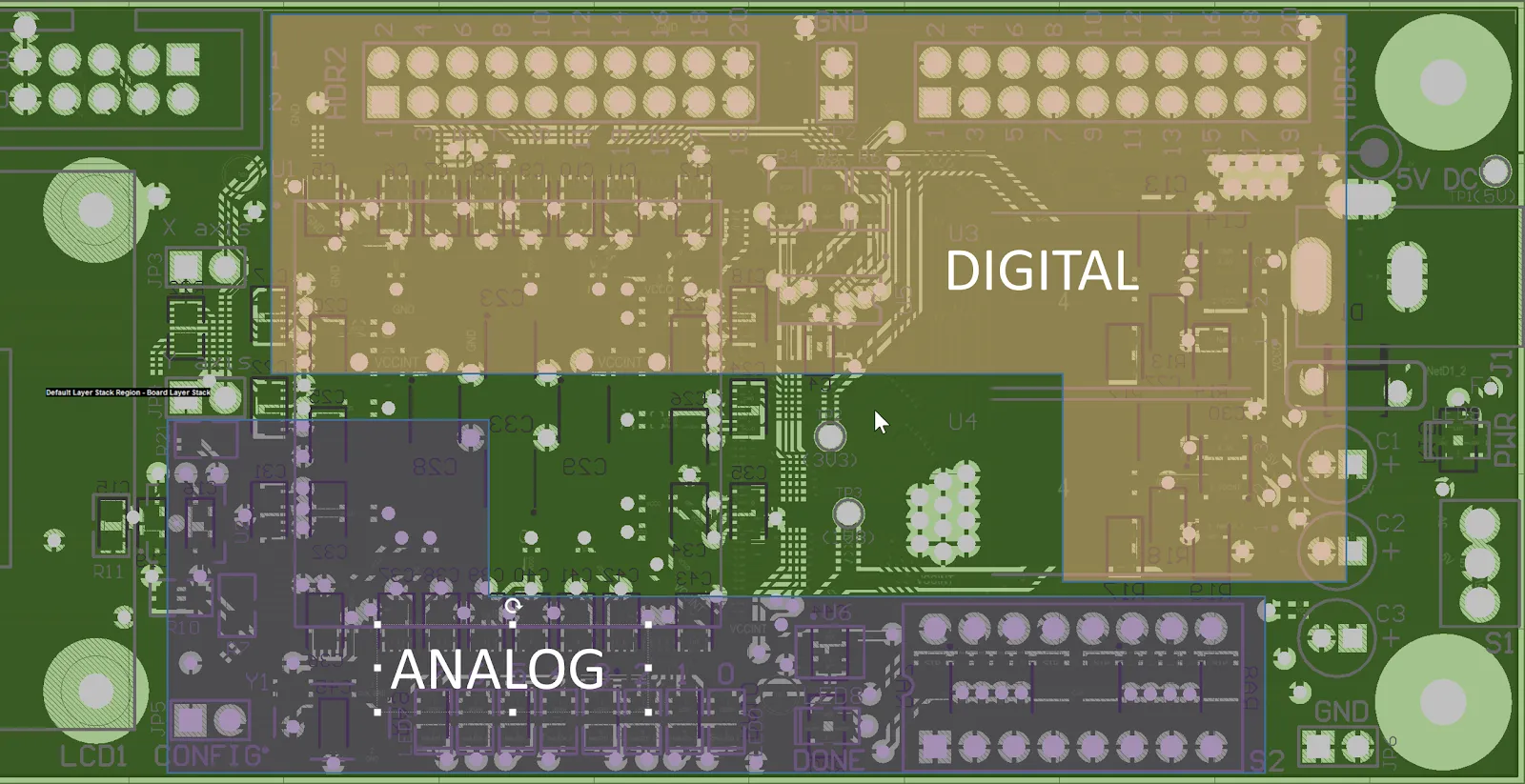
Mastering Ground Plane Partitioning: A Comprehensive Guide for Signal Integrity
Master ground plane partitioning to achieve superior PCB signal integrity in high-speed designs. This comprehensive guide covers return path optimization, impedance control, best practices, and common pitfalls—essential reading for reliable mixed-signal and RF PCBs.
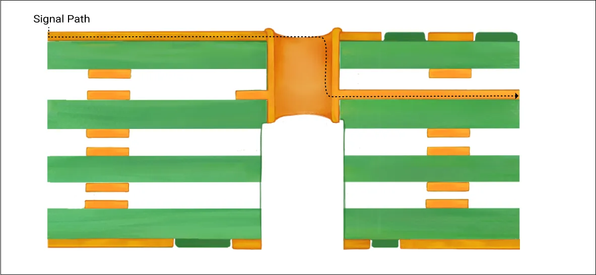
Backdrilling Design: A Beginner's Guide to Reducing Signal Reflections in PCBs
Learn PCB backdrilling for beginners to reduce signal reflections and via stub effects in multilayer boards. This guide covers basics, techniques, and best practices for hobbyists designing high-speed circuits with cleaner signals and reliable performance.
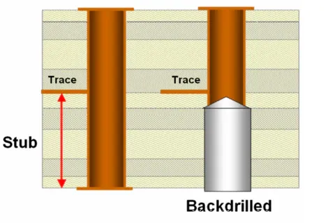
Advanced Backdrilling Design: Optimizing Stackup for High Performance PCBs
Master advanced backdrilling design and stackup optimization for high-performance PCBs. Learn how to minimize via stubs, improve signal integrity at multi-Gbps speeds, balance layer assignments, control backdrill depths, and overcome warpage for reliable high-speed designs in servers, telecom, and AI hardware.
Signal Integrity Secrets: How Backdrilling Design Optimizes Your PCB Performance
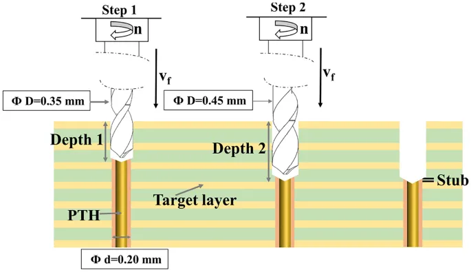
Signal integrity backdrilling removes via stubs to counter resonance and achieve impedance matching in high-frequency PCBs. This guide details technical principles, best practices, troubleshooting steps, and FAQs to support electric engineers in PCB performance optimization.


