










Designing coverlay openings the exact size of the copper pad looks clean in CAD. It is also one of the more common sources of soldering and reliability problems on flexible circuits.
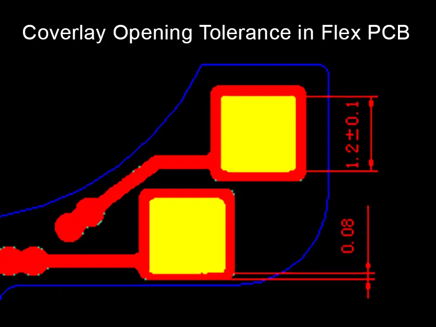
FPC coverlay opening compensation exists because the coverlay does not land with perfect registration and the adhesive does not stay perfectly still during lamination. A true 1:1 opening leaves no margin for those realities.
Why Coverlay Openings Require Compensation
Coverlay is a polyimide film with adhesive that is aligned and laminated over the flexible circuit. The openings are either pre-punched, laser-cut, or formed after lamination. None of these steps is perfect.
Registration tolerance between the coverlay and the copper pattern is typically in the range of ±0.1 mm to ±0.3 mm depending on panel size, material, and process control. Adhesive flow during the heat and pressure of lamination further reduces the effective opening size. Polyimide itself changes dimension slightly with temperature and moisture.
When these variations stack, a 1:1 opening can easily leave part of the pad covered by coverlay or adhesive. The result is incomplete solder wetting, reduced joint strength, or exposed copper where it was not intended.
Compensation—making the opening larger than the copper feature—absorbs those tolerances so the finished pad remains fully accessible.
Problems Created by True 1:1 Coverlay Openings
The most immediate issue is incomplete pad exposure. Solder paste or the soldering iron cannot reach the full copper surface. Wetting becomes inconsistent. On fine-pitch pads the problem is especially visible: one side of the pad may solder while the other remains partially masked.
Misalignment in the opposite direction leaves copper exposed outside the intended opening. That exposed copper can oxidize, create solder bridges, or become a corrosion site. In high-density areas it can also short to adjacent features if debris or flux residue is present.
Both conditions reduce first-pass yield and create latent reliability risks. A joint that looks acceptable after reflow can still fail under flexing or thermal cycling because the effective solderable area was smaller than designed.
These defects are process-dependent. A fabricator with tight registration and low-flow adhesive may survive a 1:1 design on a simple part. The same design on a larger panel or with a different material stack will fail.
Pad Coverage and Misalignment Risks in Practice
When the opening is undersized relative to the actual process variation, two failure modes dominate.
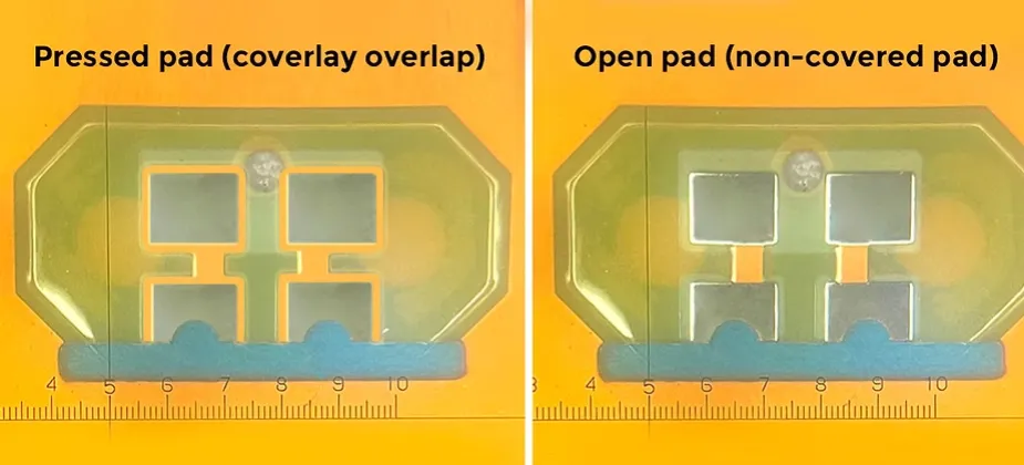
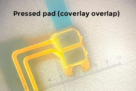
Insufficient pad coverage. Part of the copper remains under coverlay or adhesive. Solder volume is reduced. The joint may meet electrical continuity but fail mechanical pull or peel tests. On component pads this shows up as weak fillets or tombstoning tendency.
Opening shift. The entire window moves relative to the pad. One edge of the pad is covered while the opposite edge has excess exposure. The solder joint becomes asymmetric. In connector or gold-finger areas the functional contact surface can be compromised.
Both risks increase with smaller pads, tighter pitch, and larger panel sizes. Flexible PCB coverlay tolerance is not a single number; it is the combination of registration, material movement, and adhesive behavior. Designing at 1:1 ignores that stack-up.
How Fabricators Apply Opening Compensation
Most FPC manufacturers do not expect a true 1:1 opening. They apply a standard enlargement based on their process capability.
Typical compensation is 0.1 mm to 0.15 mm per side for well-controlled laser or punch processes on smaller panels. On larger panels or with higher-flow adhesives the value may rise to 0.2 mm or 0.25 mm per side. Some fabricators publish a minimum opening size relative to the copper pad; others prefer the designer to supply the already-compensated opening and then hold registration to that geometry.
The compensation is not arbitrary. It is sized so that under worst-case registration and adhesive flow the entire copper pad remains clear of coverlay. At the same time it is kept small enough that excess copper exposure stays within acceptable limits for the application.
When the designer supplies a 1:1 opening, the fabricator must either enlarge it (changing the designer's intent) or run the risk of partial coverage. Both approaches create ambiguity. Clear communication of the compensation rule removes that ambiguity.
Practical Design Approach for Coverlay Openings
The cleanest method is to design the opening larger than the copper pad by the amount the fabricator requires. For many production FPCs this means an opening that is 0.2–0.3 mm larger in both X and Y than the copper feature (0.1–0.15 mm per side).
For critical fine-pitch pads the compensation may be applied more carefully—sometimes only on the sides where registration risk is highest, or with a minimum opening size rule rather than a uniform enlargement.
Always confirm the fabricator's preferred rule before finalizing the coverlay layer. Some prefer the designer to draw the compensated opening; others prefer nominal size plus a process note and will apply the enlargement themselves. Either method works if it is explicit.
Also verify that the enlarged opening does not violate other clearances—adjacent copper, coverlay web width, or stiffener edges. Compensation that solves pad exposure can create new problems if the surrounding geometry is tight.
When 1:1 Might Still Be Used
There are limited cases where a near-1:1 opening is intentional. Very large pads with generous surrounding space can tolerate small misalignment. Some controlled-impedance or tightly spaced features may restrict how much enlargement is possible. In those situations the designer must accept tighter process control, higher inspection, or a higher risk of partial coverage.
For the majority of component pads, test points, and connector fingers, compensation remains the lower-risk choice. The slight increase in opening size is almost always preferable to the soldering and reliability issues that follow from insufficient exposure.
Engineering Takeaway
FPC coverlay openings are not designed at true 1:1 size because registration tolerance, adhesive flow, and material movement make perfect alignment impossible. A 1:1 opening frequently results in partial pad coverage or unwanted copper exposure.
Proper FPC coverlay opening compensation—typically 0.1 to 0.15 mm per side or according to the fabricator's process—ensures the pad remains fully solderable under real manufacturing variation. Treating flexible PCB coverlay tolerance as a design input rather than an afterthought removes one of the more persistent sources of assembly defects on flexible circuits.






