Embedded Passives
Embedded passives represent a key advancement in printed circuit board (PCB) design, where components such as resistors, capacitors, and inductors are integrated directly into the substrate layers rather than mounted on the surface. This approach minimizes board space, enhances electrical performance, and reduces parasitic effects that can degrade signal integrity in high-frequency applications. For engineers and designers searching for information on embedded passives, this tag serves as a comprehensive resource, offering insights into how these technologies enable more compact, reliable, and efficient electronic systems. One of the primary benefits of embedded passives is their role in supporting miniaturization trends across industries like consumer electronics, telecommunications, and automotive systems. By embedding these components, designers can achieve higher component density without compromising functionality, which is particularly valuable in space-constrained environments such as smartphones, wearables, and IoT devices. Practical applications include improving power distribution networks, filtering noise in RF circuits, and optimizing impedance matching in multilayer boards. Best practices for implementation involve selecting appropriate dielectric materials, conducting thorough simulations to predict performance, and collaborating with manufacturers experienced in advanced lamination processes to ensure yield and reliability. Understanding embedded passives also involves addressing challenges like thermal management and cost implications during the design phase. Engineers can mitigate these by incorporating tools for electromagnetic modeling and adhering to standards such as IPC-2316 for design guidelines. This tag compiles articles that delve into these topics, providing case studies and step-by-step tutorials to help you apply these concepts in real-world projects. Browsing the linked content here can offer deeper technical details and innovative strategies tailored to your specific PCB challenges.
Technical Articles
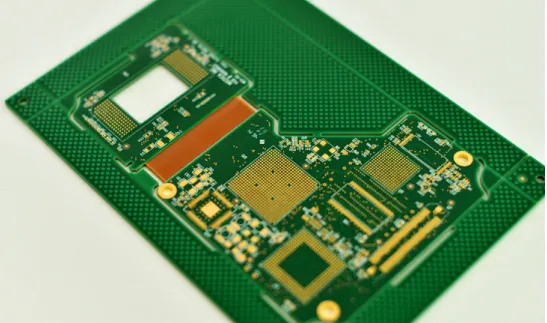
Embedded Resistors and Capacitors in PCB Manufacturing
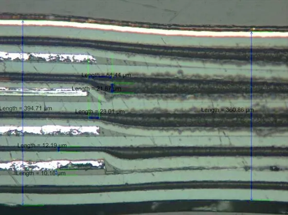
Embedded Passives in 8 Layer PCBs: Integration and Performance Benefits

Beyond the Basics: Advanced Automotive PCB Design Techniques
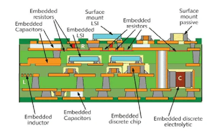
High Frequency Design: Optimizing Performance with Buried Resistors
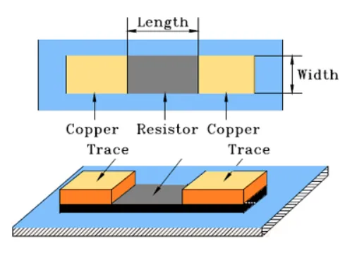
Tolerance Tightrope: Achieving Precision with Buried Resistors in Critical Applications
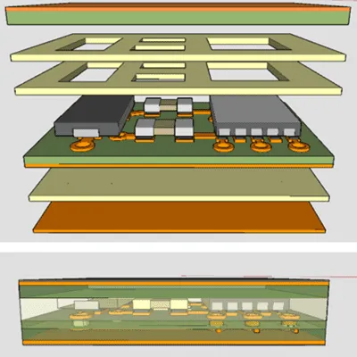
Prototyping Embedded Component PCBs: A Beginner's Guide