


 00:53
EMI
Electromagnetic interference, commonly known as EMI, poses a significant challenge in the design and operation of printed circuit boards and electronic systems. This tag encompasses a range of topics related to understanding, mitigating, and managing EMI to ensure reliable performance in various applications. For engineers, hobbyists, and professionals searching for EMI solutions, the content here provides essential knowledge on how electromagnetic waves from sources like power lines, radio frequencies, or nearby devices can disrupt signal integrity, leading to malfunctions or compliance failures. Key aspects covered include the fundamentals of EMI sources, such as radiated and conducted interference, and their impact on sensitive components like microcontrollers, sensors, and communication modules. Practical strategies for EMI reduction are highlighted, including effective PCB layout techniques such as multilayer stackups, proper trace routing to minimize loop areas, and the use of ground planes for better shielding. Best practices also extend to component selection, like choosing low-EMI capacitors or ferrite beads, and implementing filtering methods to suppress noise at the source. In real-world scenarios, addressing EMI is crucial for industries ranging from consumer electronics to automotive and aerospace, where regulatory standards like FCC or CISPR must be met to avoid costly redesigns or product recalls. By applying these insights, designers can enhance system robustness, improve signal quality, and accelerate time-to-market. The articles associated with this EMI tag delve into case studies, simulation tools, and troubleshooting guides that offer step-by-step approaches to diagnose and resolve interference issues, helping you implement effective solutions tailored to your projects.
Video Guide
-
00:53
Technical Articles
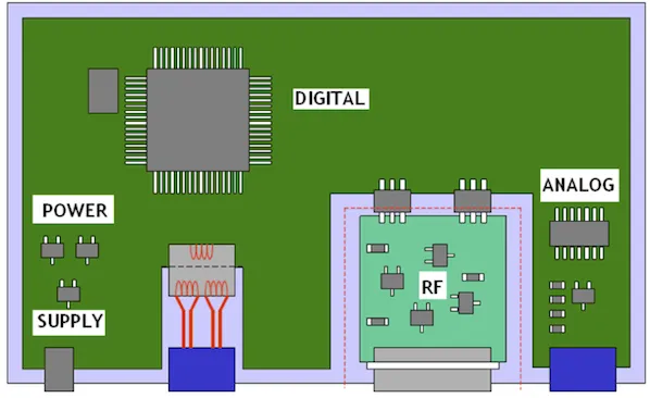
EMC and Protection Design for Modular Power Peripheral Circuits
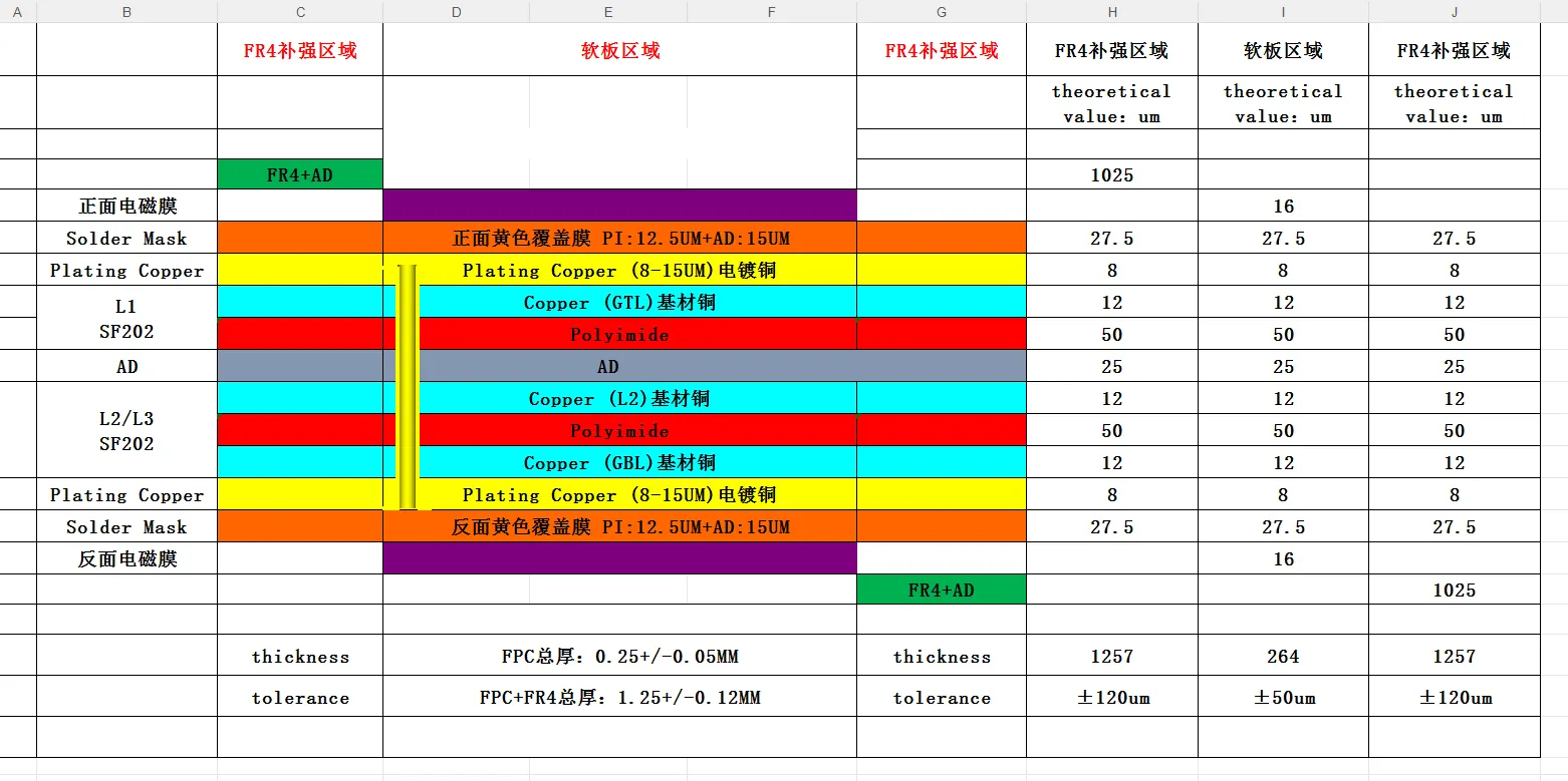
FPC Stiffener Design Rules: Avoiding Common DFM Roadblocks
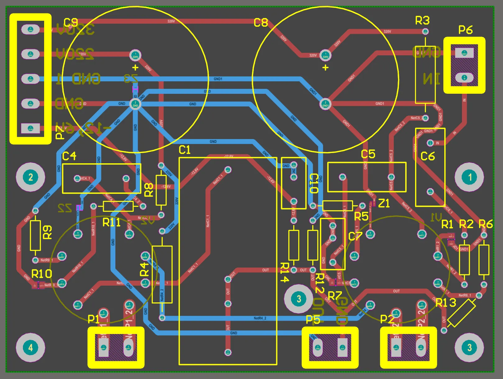
Improve Your Designs with the Best PCB Grounding Techniques
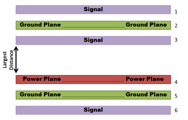
The Art of Layering: Signal Layer Strategies for PCB Success
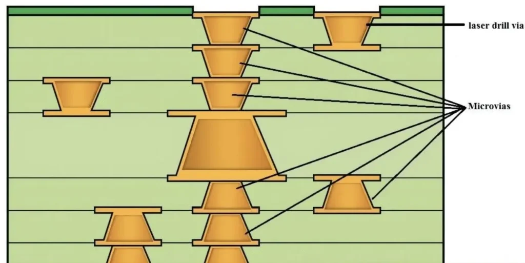
Microvia Design for EMI Reduction
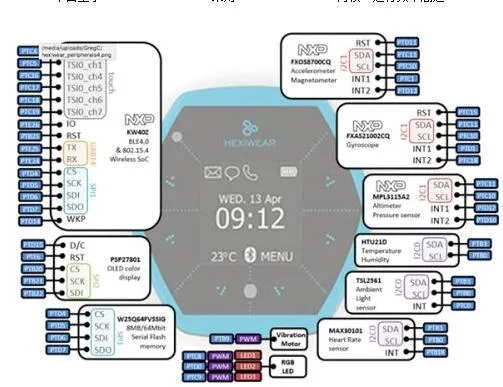
Advanced PCB Design & Manufacturing for Medical Electronics: Reliable Wearable, Portable, and IoT Solutions
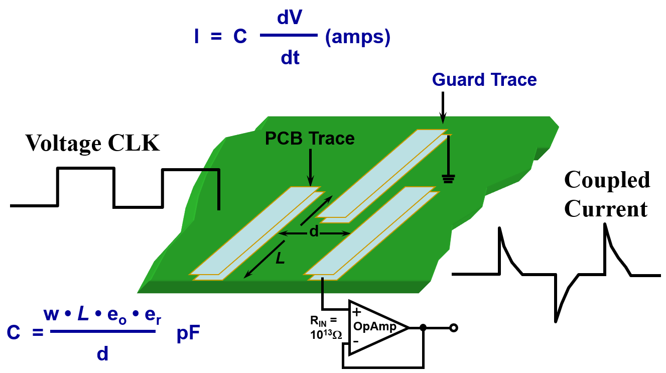
Reducing EMI in PCB Prototyping: Shielding Techniques and Grounding Strategies
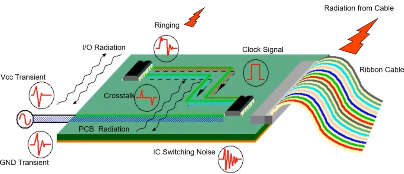
EMI and EMC Compliance 101 for PCB Designers
CS114 Calibration and Test Methods
Analyzing Antennas from Oscillator Equations
How Cloud Security Differs from Traditional Security
100 Oscilloscope Basics Q&A

Common Network Information Security Attributes
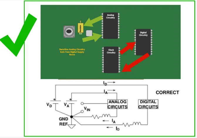
The Impact of Component Orientation on PCB Signal Integrity and Performance
PCB Prototyping Assembly: Optimizing for Electromagnetic Compatibility (EMC)
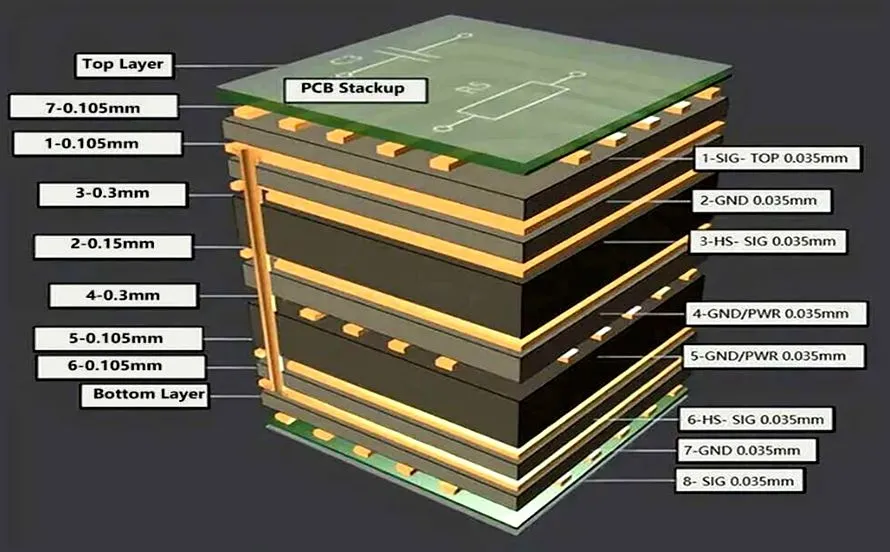
Unleashing PCB Performance: A Guide to Asymmetrical Stackup Design
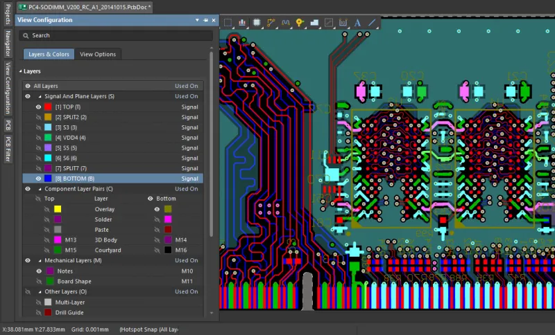
The Role of Simulation in PCB Design: Predicting Performance and Avoiding Problems
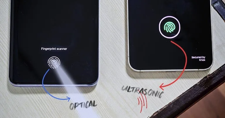
Ultrasonic Sensor PCB Design and Integration Guide: Comparison with Optical Sensors, Installation, Drivers, and Harsh-Environment Performance
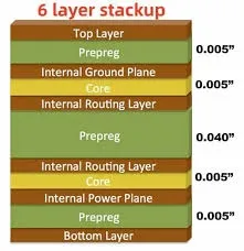
6 Layer PCB Design Guidelines for EMI/EMC Compliance


