This double-sided flexible PCB measured 9.61 mm × 8.88 mm and was specified with a polyimide base, 1/1 oz copper, yellow coverlay, ENIG finish, laser outline, and double-sided electromagnetic shielding film. The fabrication package also included an FR4 stiffener whose outline matched the board perimeter exactly and contained no clearance openings. During CAM review the combination of FPC stiffener design rules, ultra-thin stack-up targets, and incomplete via-pad definitions immediately triggered a process-capability assessment. The central question was whether the supplied stiffener geometry and 0.15 mm finished thickness could be produced repeatably without assembly interference or lamination instability.
The engineering evaluation focused on three linked observations drawn directly from the customer data and drill files. First, the FR4 stiffener outline was identical to the board outline, creating a predictable risk of edge protrusion after registration and adhesive cure. Second, the stiffener lacked relief holes, so attachment would cover existing plated and non-plated openings. Third, the requested 0.15 mm total thickness with 50 µm dielectric plus dual EMI film exceeded both material availability and stable press capability. Each observation was verified against process windows before any production release could be authorized.
FPC Stiffener Outline Pull-Back and Clearance Hole Limits
The customer FPC stiffener layer was drawn to the same finished dimensions as the flex outline. In practice, adhesive flow, registration tolerance, and the slight expansion of FR4 during lamination routinely produce a net positive offset of 0.10–0.20 mm at the perimeter. When the stiffener is the same size as the board ( #FPC-20260516-042 ), this offset causes the FR4 edge to overhang the flex contour. The resulting assembly interference can prevent proper seating in the next higher-level package or create local stress concentrations that initiate coverlay cracking.
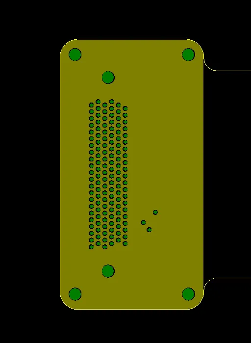
Figure 1: the FR-4 stiffener's outline is same as board outline
Equally critical was the absence of clearance (relief) holes in the stiffener. The drill file contained openings of 3.175 mm / 0.9 mm and 0.38 mm. Without corresponding larger openings in the FR4, the stiffener would permanently cover these holes after bonding. Covered holes eliminate subsequent electrical access, prevent probe contact during flying-probe test, and can trap flux or moisture. Process data from prior flex-stiffener programs show that even a 0.1 mm radial shortfall in relief diameter is sufficient to leave residual FR4 covering the copper pad annulus.
| Stiffener Feature | Customer Data | Typical Capability Window | Engineering Assessment |
|---|---|---|---|
| Outline relation to board | Identical | 0.10–0.20 mm pull-back | Protrusion risk after cure |
| 3.175 / 0.9 mm hole relief | None | 3.5 / 1.2 mm minimum | Complete coverage if unchanged |
| 0.38 mm hole relief | None | Optional (small diameter) | No relief required |
| Registration tolerance | Not stated | ±0.075 mm typical | Amplifies outline mismatch |
The recommended corrective action followed established FPC design rules: shrink the stiffener outline by 0.15 mm on all sides and open clearance holes of 3.5 mm / 1.2 mm at the larger openings while leaving the 0.38 mm openings without relief. These values provide a manufacturing margin that absorbs adhesive squeeze-out and laser-cut edge variation while preserving structural reinforcement over the majority of the flex area.
EMI Shielding Film and FPC Stackup Thickness Calculation
Parallel to the stiffener geometry issue, the stack-up definition required a 50 µm dielectric, double-sided electromagnetic film, and a finished thickness of 0.15 mm. Measurement of the supplied material call-out showed that the base polyimide plus two coverlay layers already approach 0.12–0.13 mm before any EMI film is applied. Each EMI film contributes an additional cured thickness of approximately 40–60 µm; the dual-film construction therefore drives the theoretical minimum well above 0.20 mm under normal vacuum-press conditions.
Process capability data for flexible constructions thinner than 0.20 mm become statistically unstable once dual EMI films are introduced. The films require a minimum pressure and temperature dwell to achieve reliable adhesion; reducing that pressure to force a 0.15 mm total thickness risks incomplete bonding, interfacial voids, and local thickness variation that routinely exceeds ±0.03 mm. IPC-6013 Class 2 thickness tolerance guidance already permits ±10 % on thin flex circuits; a 0.15 mm nominal leaves essentially no remaining process window once material lot variation and press-to-press differences are included.
In addition, the exact DuPont material combination specified for the 50 µm dielectric and compatible EMI film was not available in the required gauge. Continuing with an unproven substitute under the original thickness target would have introduced uncontrolled variables in both adhesion and dimensional stability. The only controllable path was to redefine the total stack-up around a material set that could be pressed repeatably.
| Stack-up Element | Requested Value | Achievable with SF202 | Capability Margin |
|---|---|---|---|
| Finished thickness | 0.15 mm | 0.25 ± 0.05 mm | Stable |
| Dielectric | 50 µm | SF202 compatible | Within window |
| EMI film (double) | Required | Included | Primary thickness driver |
| Material source | DuPont | Shengyi SF202 | Substitution accepted |
After confirming material unavailability, the process team evaluated Shengyi SF202 as the base flexible dielectric. Cross-section coupons from previous SF202 lots demonstrated consistent thickness and good compatibility with the electromagnetic shielding films already qualified on other programs. The revised build sequence produced a measured total thickness of 0.25 mm ± 0.05 mm after full cure. This window sits inside the capability of the vacuum press and subsequent laser-outline and flying-probe operations while still satisfying IPC-6013 thickness requirements for circuits of this size.
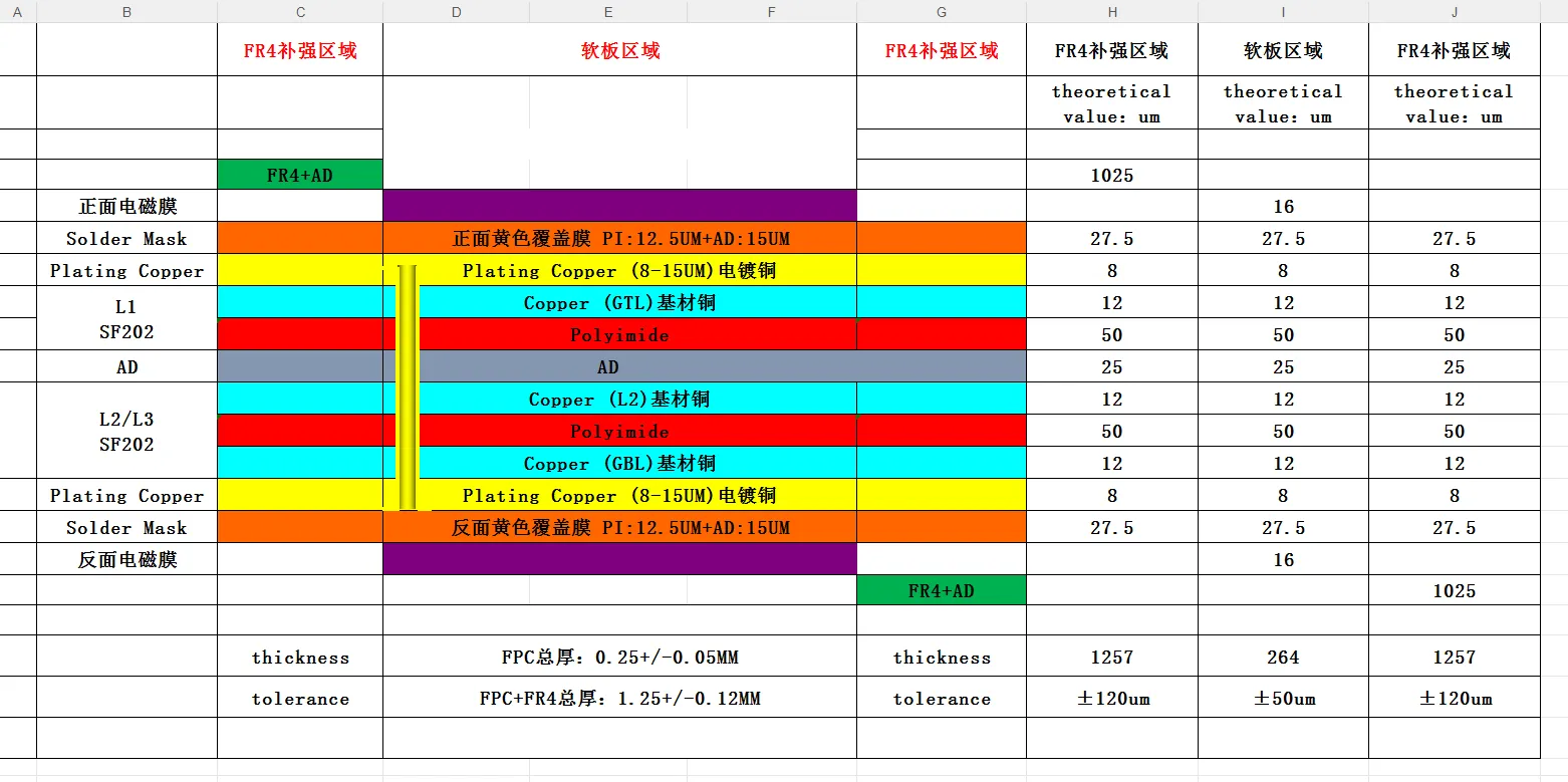
Figure 2: stackup showing FPC+EMI film total thickness in 0.25+/-0.05mm
Via Pad Completeness and PTH versus NPTH Classification
A secondary but still production-critical observation concerned two holes that appeared in the drill file as plated-through features yet carried copper pads on only the reverse side. Under standard plating chemistry these openings would emerge as non-plated holes because the front-side surface lacked both a pad and an opening in the coverlay. The resulting electrical discontinuity would violate the design intent if the holes were intended to interconnect both sides.
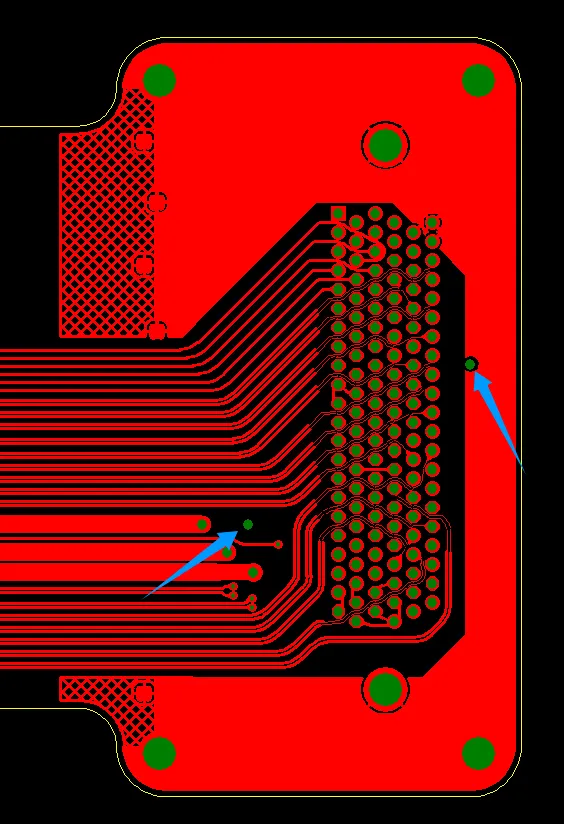
Figure 3: there are 2 holes (indicated by the arrow) only have via pad on the bottom layer
The corrective action was straightforward: add matching via pads and coverlay openings on the front side so that both holes could be processed as plated-through. File confirmation was obtained before any panelization proceeded. This adjustment restored plating continuity without altering hole diameter or position and eliminated the risk of intermittent open circuits that would otherwise appear only after final assembly.
Physical Process Windows for Stiffener Bonding and Thin Flex Lamination
FR4 stiffener bonding on flexible circuits operates inside a relatively narrow process window. Adhesive thickness, cure temperature, and registration accuracy must be controlled simultaneously. When the Flexible PCB stiffener outline is identical to the flex contour, even a 0.05 mm registration shift combined with adhesive squeeze-out produces measurable overhang. IPC-A-600 acceptability criteria for edge definition on flexible circuits treat such overhang as a potential workmanship defect once it exceeds the nominal board outline.
Lamination of dual EMI films imposes additional constraints. The films must reach a minimum temperature and pressure to achieve metallurgical and adhesive continuity; yet excessive pressure on an ultra-thin stack risks copper wrinkling and dielectric thinning. The original 0.15 mm target left no margin for either condition. By moving to the 0.25 mm ± 0.05 mm SF202-based construction, both the stiffener bond line and the EMI film interfaces could be held within established capability indices.
The combined process flow therefore became:
- SF202 base + copper imaging
- Coverlay and dual EMI film application
- Vacuum press to 0.25 mm ± 0.05 mm
- Laser outline with stiffener pull-back of 0.15 mm
- Stiffener clearance drilling (3.5 / 1.2 mm at major holes)
- FR4 stiffener bonding and final flying-probe test
Each step was verified against prior process capability studies before the revised data package was released for production.
Capability Verification Through Cross-Section and Dimensional Checks
Prototype panels were built to the adjusted stack-up and stiffener geometry. Cross-section analysis confirmed that the total thickness after EMI film cure remained inside 0.25 mm ± 0.05 mm across multiple panel locations. Adhesion of the electromagnetic film to the SF202 coverlay met the minimum peel-strength values established for production lots. Dimensional inspection of the stiffener outline verified a consistent 0.15 mm pull-back relative to the laser-cut flex edge, and the 3.5 / 1.2 mm clearance holes fully exposed the corresponding copper pads.
Electrical continuity testing of the two previously incomplete vias demonstrated plated barrels on both sides once the front-side pads and openings were added. No opens or high-resistance readings were recorded. These results established that the revised FPC stiffener design rules and stack-up thickness produced a stable, repeatable manufacturing window.
| Verification Item | Method | Result | Capability Status |
|---|---|---|---|
| Finished thickness | Cross-section | 0.25 ± 0.05 mm | Inside window |
| Stiffener pull-back | Optical CMM | 0.15 mm nominal | Consistent |
| Clearance hole exposure | Visual + probe | Full pad access | Acceptable |
| PTH continuity | Flying probe | No opens | Confirmed |
Approved Manufacturing Window and Release Decision
The final engineering disposition retained the dual EMI film and FR4 stiffener while implementing three controlled adjustments: (1) stiffener outline reduced by 0.15 mm, (2) clearance holes of 3.5 mm / 1.2 mm at the larger openings, and (3) total stack-up thickness of 0.25 mm ± 0.05 mm using Shengyi SF202. These changes restored a usable process window for both stiffener bonding and thin-flex lamination without altering the functional copper pattern or shielding performance.
The case illustrates that FPC stiffener design rules are not merely geometric preferences; they define the boundary between a design that can be manufactured at stable yield and one that will generate recurring assembly interference or thickness variation. By quantifying the capability margins for outline pull-back, relief diameter, and EMI-film stack-up thickness, the engineering team converted an otherwise non-manufacturable data package into a production-ready construction.
FAQ
Q1: Why must FR4 stiffener outlines on flex PCBs incorporate a deliberate pull-back?
A1: Adhesive flow, registration tolerance, and FR4 expansion during cure routinely produce a net positive offset of 0.10–0.20 mm. An identical outline therefore results in edge protrusion after bonding. A 0.15 mm pull-back absorbs these process variations and keeps the stiffener inside the flex contour, satisfying both dimensional and IPC-A-600 edge-definition criteria.
Q2: How large should FPC stiffener clearance holes be relative to the plated openings they protect?
A2: Clearance diameter must exceed the finished hole by enough to accommodate registration error and adhesive squeeze-out. In this case a 3.175 / 0.9 mm hole required a 3.5 / 1.2 mm relief. Smaller openings such as 0.38 mm may be left without relief when structural coverage is prioritized and electrical access is not required after stiffener attachment.
Q3: Why does dual EMI shielding film prevent a 0.15 mm finished thickness on flexible circuits?
A3: Each EMI film contributes 40–60 µm of cured thickness. Combined with base dielectric and coverlay, the theoretical minimum already exceeds 0.20 mm under normal press conditions. Forcing 0.15 mm requires reduced pressure that compromises adhesion and produces thickness variation outside IPC-6013 tolerance bands.
Q4: When is material substitution acceptable for an EMI-shielded FPC stack-up?
A4: Substitution is acceptable when the original material is unavailable in the required gauge and the replacement has been previously qualified for thickness control, adhesion, and EMI-film compatibility. In this evaluation Shengyi SF202 provided a documented process window of 0.25 mm ± 0.05 mm while preserving the functional shielding layers.
Q5: What risk arises when a drill file shows plated holes but pads exist on only one side of a flex circuit?
A5: Standard electroless and electrolytic plating will not deposit copper on a surface that lacks both a pad and a coverlay opening. The hole therefore emerges non-plated, creating an open circuit if interconnection was intended. Adding the missing pad and opening restores PTH continuity without changing hole diameter or position.
Q6: How do FPC stiffener design rules interact with overall process capability?
A6: Stiffener outline pull-back and clearance diameter define the geometric boundary of the process window. When these rules are violated, even a well-controlled lamination and laser-cut process will produce assembly interference or covered holes. Observing the rules restores a manufacturable margin that can be held across production lots.