 00:58
00:58
High Current PCB
High current PCBs are specialized printed circuit boards engineered to handle substantial electrical loads, often exceeding 10 amps per trace, without compromising performance or safety. These boards are essential in applications where power delivery is critical, such as in power supplies, motor controllers, electric vehicle chargers, and industrial automation systems. For engineers and designers searching for information on high current PCB design, this tag serves as a comprehensive resource, offering insights into optimizing layouts for minimal resistance, enhanced thermal dissipation, and reliable operation under demanding conditions. Key considerations in high current PCB development include selecting appropriate copper thicknesses, typically 2 oz or higher, and calculating trace widths using tools like the IPC-2221 standard to prevent overheating and voltage drops. Practical applications often involve multilayer boards with dedicated power planes to distribute current evenly, reducing electromagnetic interference and improving signal integrity. Best practices emphasize incorporating thermal vias, heat sinks, and solder mask openings for better heat management, while avoiding common pitfalls like insufficient clearance between high current paths and sensitive components. By addressing these elements, designers can achieve robust boards that meet regulatory standards and extend product lifespan. This tag aggregates articles that delve into real world examples, simulation techniques, and case studies, providing actionable guidance for both novice and experienced professionals. Whether you are troubleshooting a high power prototype or scaling up for production, the content here equips you with the knowledge to implement effective solutions tailored to your project's requirements.
Video Guide

Technical Articles
FR4 PCB Thermal Vias: Placement and Design Guidelines
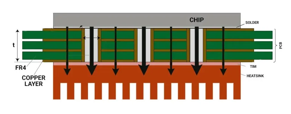
FR4 PCB Thermal Via Design for High-Power Components

FR4 PCB Resin Void: Causes and Manufacturing Prevention
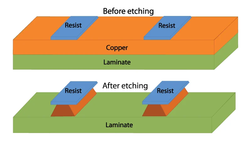
FR4 PCB Etching Undercut: Causes and Process Control
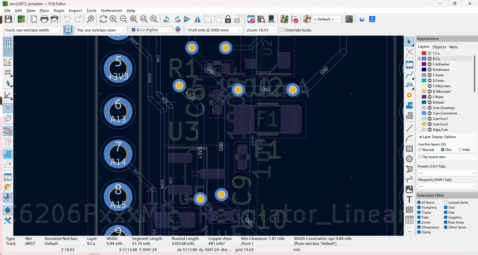
Working with Copper Zones in KiCad: Ground Planes and Design Guidelines
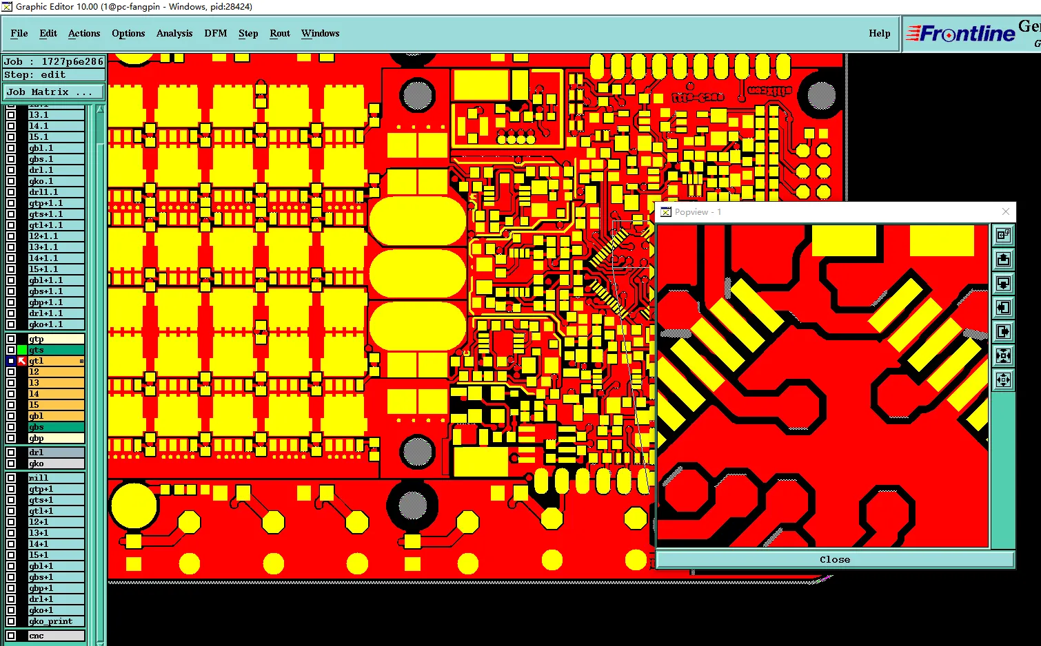
How DFM Prevented Heavy Copper Etch Failures in Multilayer PCB
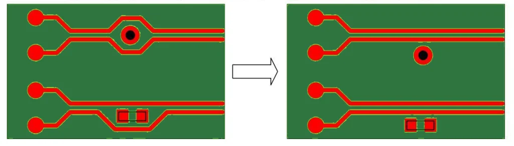
Mastering Metal Core PCB Routing: Tips and Tricks for Optimal Performance
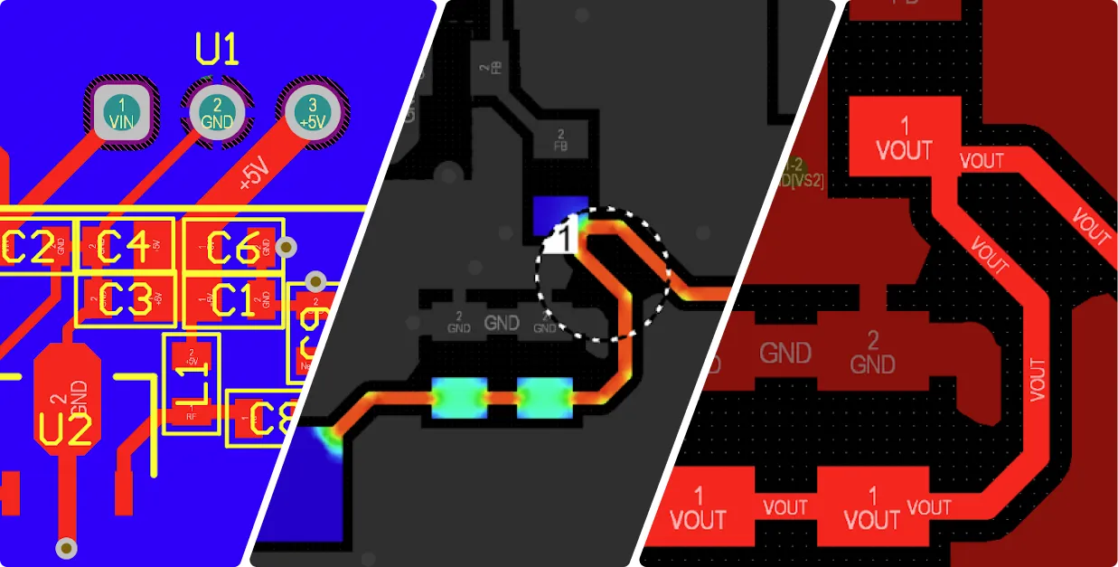
Power Distribution PCB Design
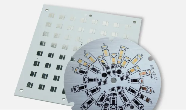
How to Choose the Right Thickness for Your Metal Core PCB
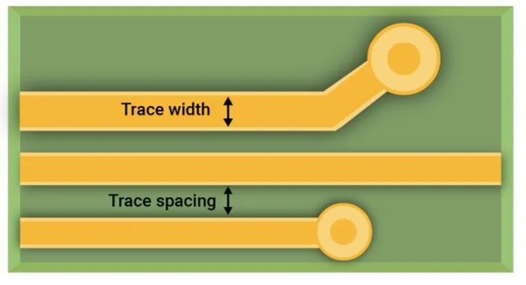
The Impact of PCB Trace Width on Solar Inverter Efficiency: A Detailed Analysis
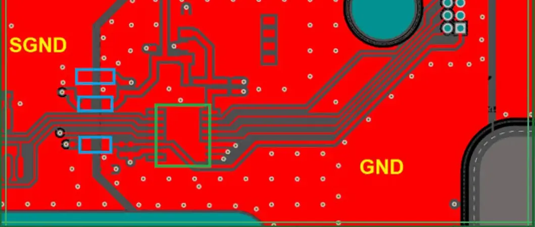
Copper Pour in Power Planes: Maximizing Current Capacity and Voltage Stability
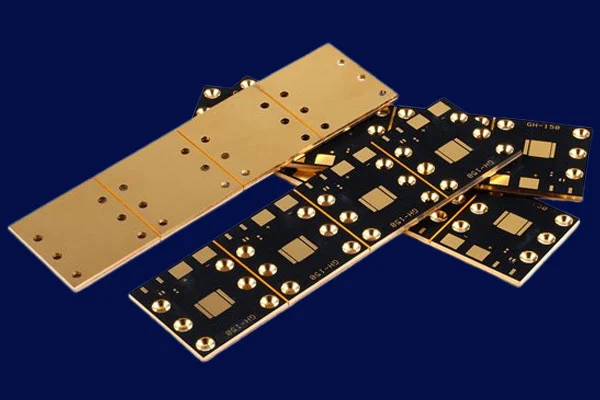
Metal Core PCBs: Enhancing Heat Dissipation with Double Sided Designs
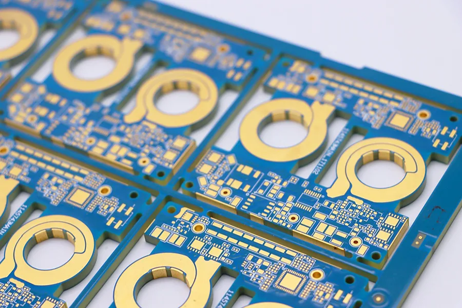
Heavy Copper PCBs: Advantages of Using Double-Sided Designs

Actuator Technology for Process Automation

The Art of Vending Machine PCB Layout: Optimizing for Signal Integrity and EMC
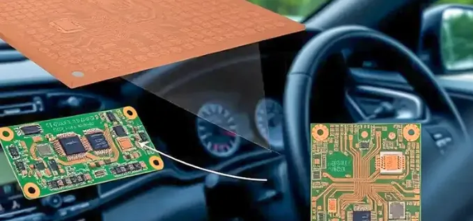
Heavy Copper PCB Applications: Powering High-Performance Electronics
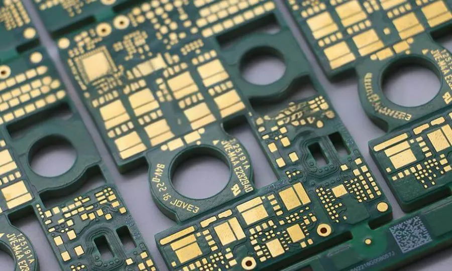
Heavy Copper PCB Design: Principles, Rules, and Best Practices
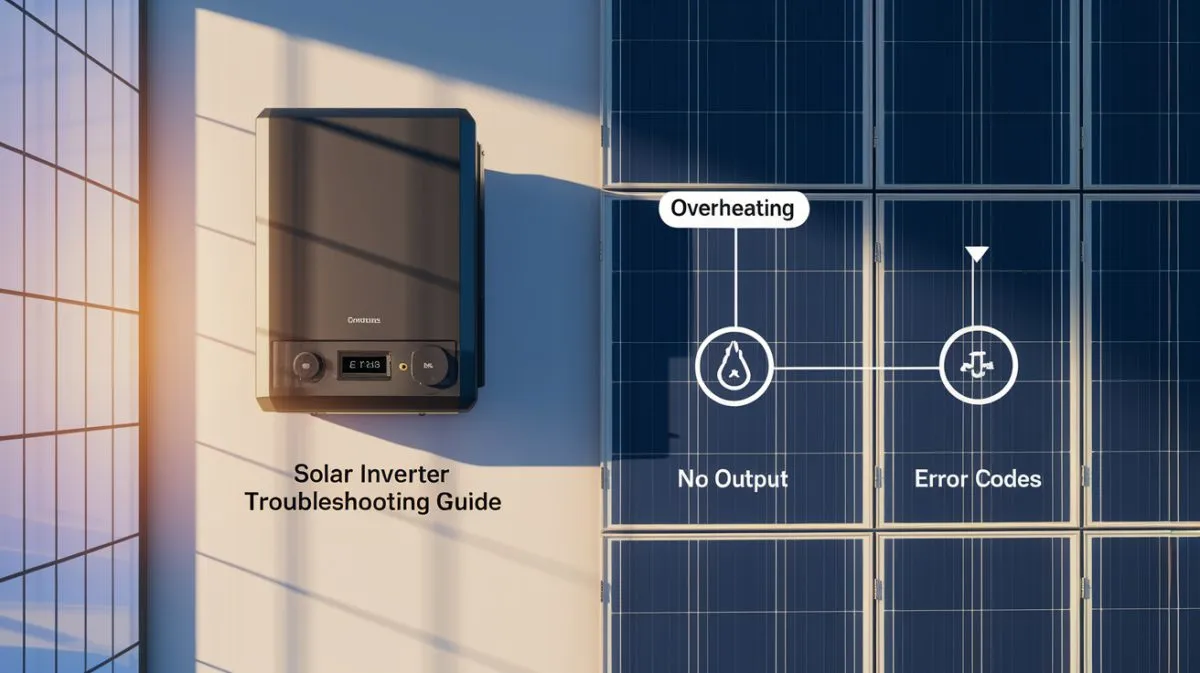
Troubleshooting Common Issues in Solar Inverter PCBs: A Practical Approach
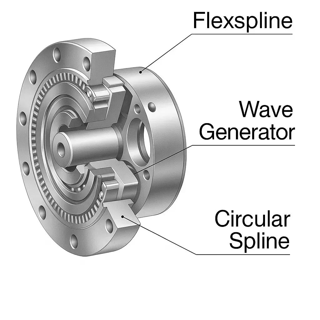
RV vs Harmonic Reducers: Principles and Trade-offs