High-Frequency PCB
High-frequency PCBs are essential components in modern electronics, enabling reliable performance in applications where signals operate at gigahertz levels or higher. These specialized printed circuit boards are designed to handle rapid signal transitions, minimizing issues like signal attenuation, crosstalk, and electromagnetic interference that can degrade system efficiency. Engineers and designers often turn to high-frequency PCB resources to address challenges in fields such as telecommunications, radar systems, wireless networks, and high-speed computing. Understanding the fundamentals of high-frequency PCB design starts with selecting appropriate materials, such as low-loss dielectrics like PTFE or Rogers laminates, which maintain signal integrity over extended distances. Key best practices include controlled impedance routing, where trace widths and spacing are precisely calculated to match the characteristic impedance of the transmission lines. Ground planes and via structures must be optimized to prevent unwanted resonances, while simulation tools like HFSS or CST can validate designs before prototyping. Practical applications extend to 5G infrastructure, where these PCBs support faster data rates, and in automotive radar for advanced driver-assistance systems, ensuring low latency and high reliability. For those troubleshooting common pitfalls, such as skin effect losses or parasitic capacitances, detailed guides on multilayer stackups and shielding techniques offer actionable solutions. By delving into these topics, professionals can enhance their designs to meet stringent performance standards, reducing time to market and improving overall product quality. Browsing through the articles tagged under High-Frequency PCB provides in-depth explorations of these concepts, equipping you with the knowledge to tackle real-world engineering demands effectively.
Technical Articles
High-Performance PCB Assembly: Key Design Considerations 2026
HDI PCB Materials Selection for High Frequency Applications
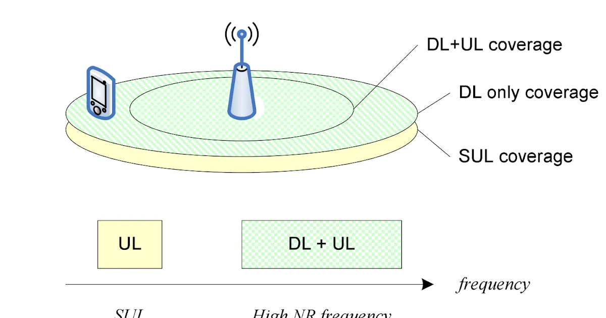
5G Super Uplink: Definition and Principles

South Korea Dedicated 5G Spectrum: Status and Outlook
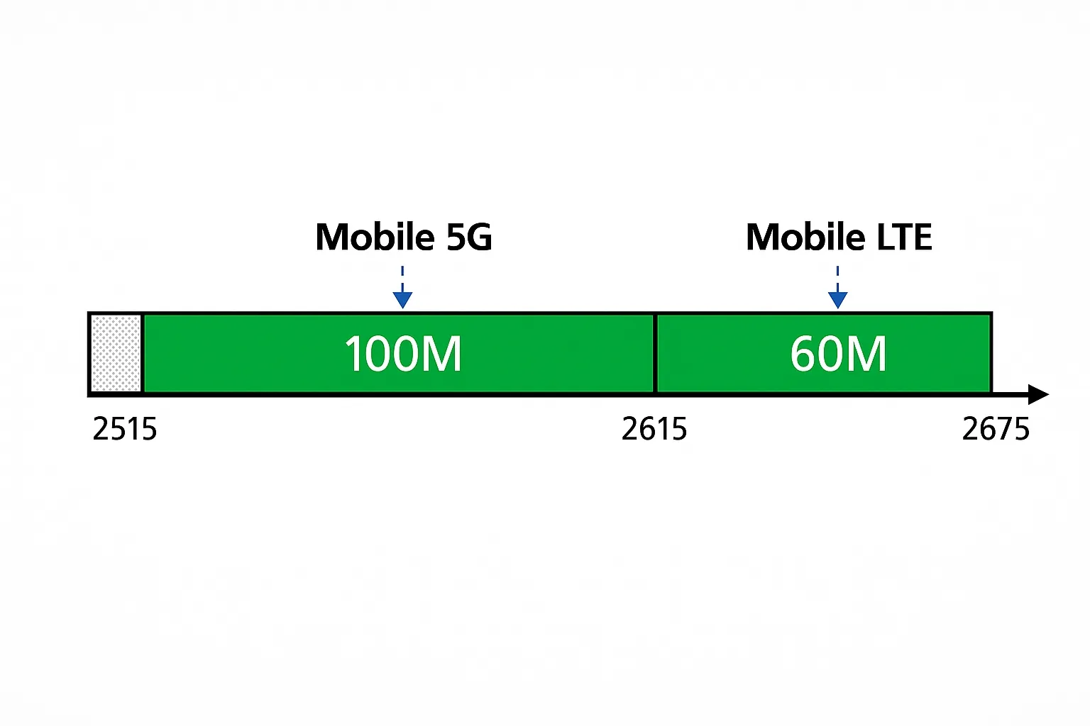
3CC Carrier Aggregation in 5G-A: Engineering and Manufacturing Implications for High-Performance Electronics
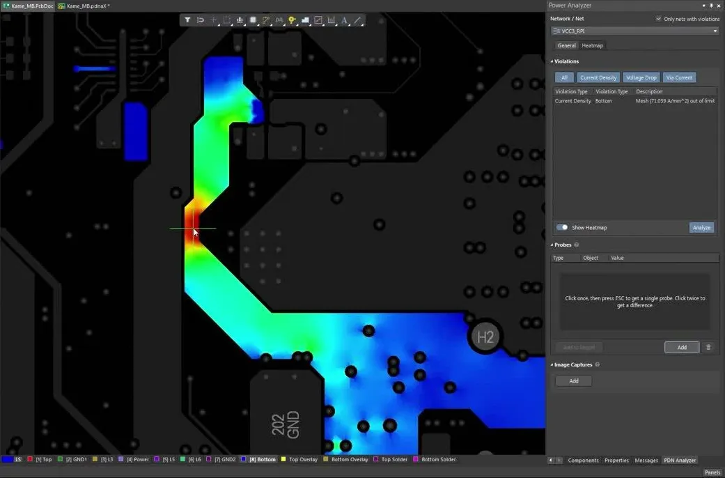
Advanced Material Selection for PCB: Optimizing Performance and Reliability using Software
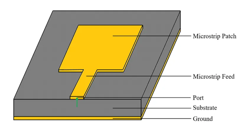
High Frequency PCB Layout Techniques for Satellite Communication Systems
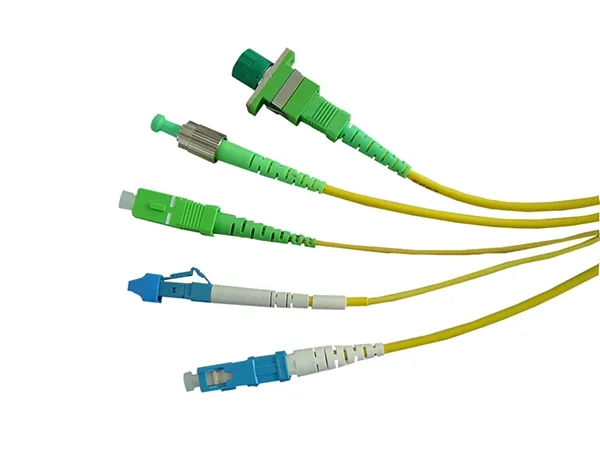
Advanced PCB Design Strategies for Fiber Optic Modules and LiFi Wireless Communication Systems
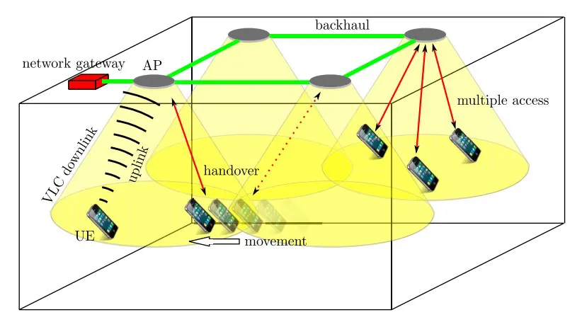
LiFi Visible Light Communication Explained
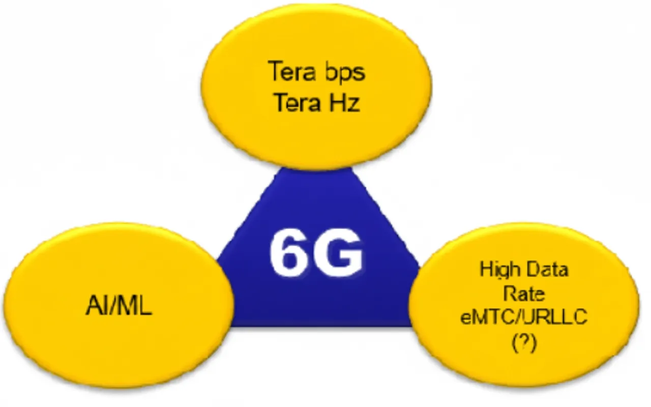
6G Mobile Communications: PCB Design, 3D Integration, and Manufacturing Challenges for THz, AI-Native, and Massive MIMO Systems
Beyond FR 4: Exploring Advanced PCB Materials for High Performance LED Lighting
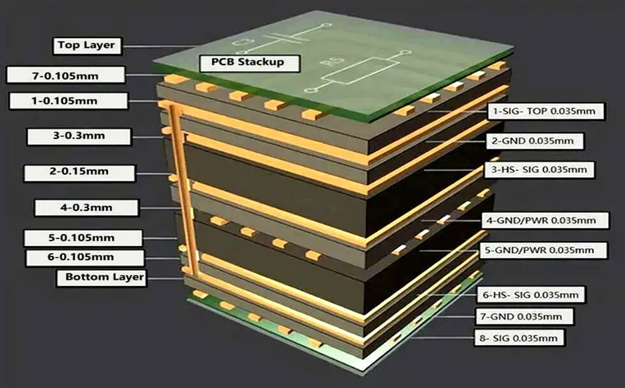
Unlocking the power of 5G Through PCB Design
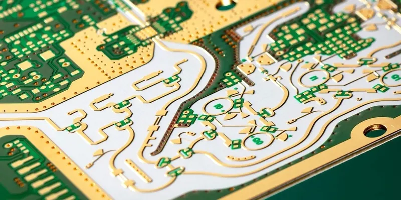
Conformal Coatings for High-Frequency PCBs: Balancing Protection and Signal Integrity
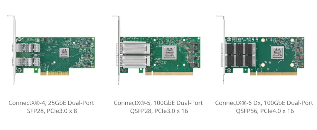
RoCE v2 Core Technical Principles
5G RedCap Technology Explained
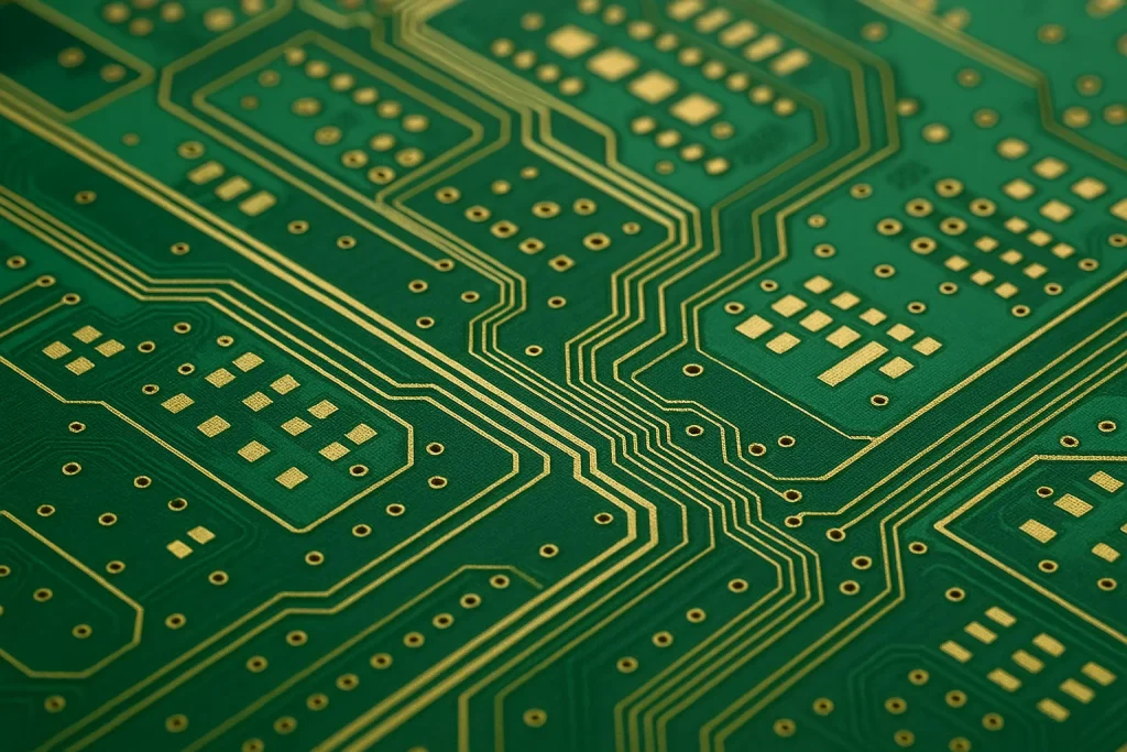
High Frequency PCB Routing Techniques: Minimizing Signal Loss and Interference
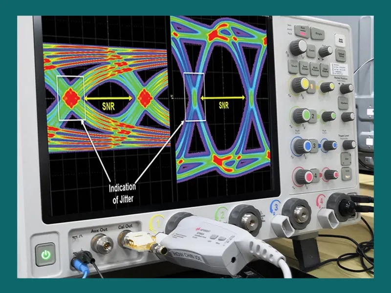
Smart Grid PCB Materials: Choosing the Right Substrate for Performance
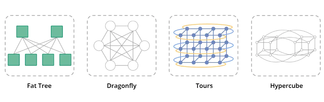
InfiniBand Networks: HDR and IB Technology Overview