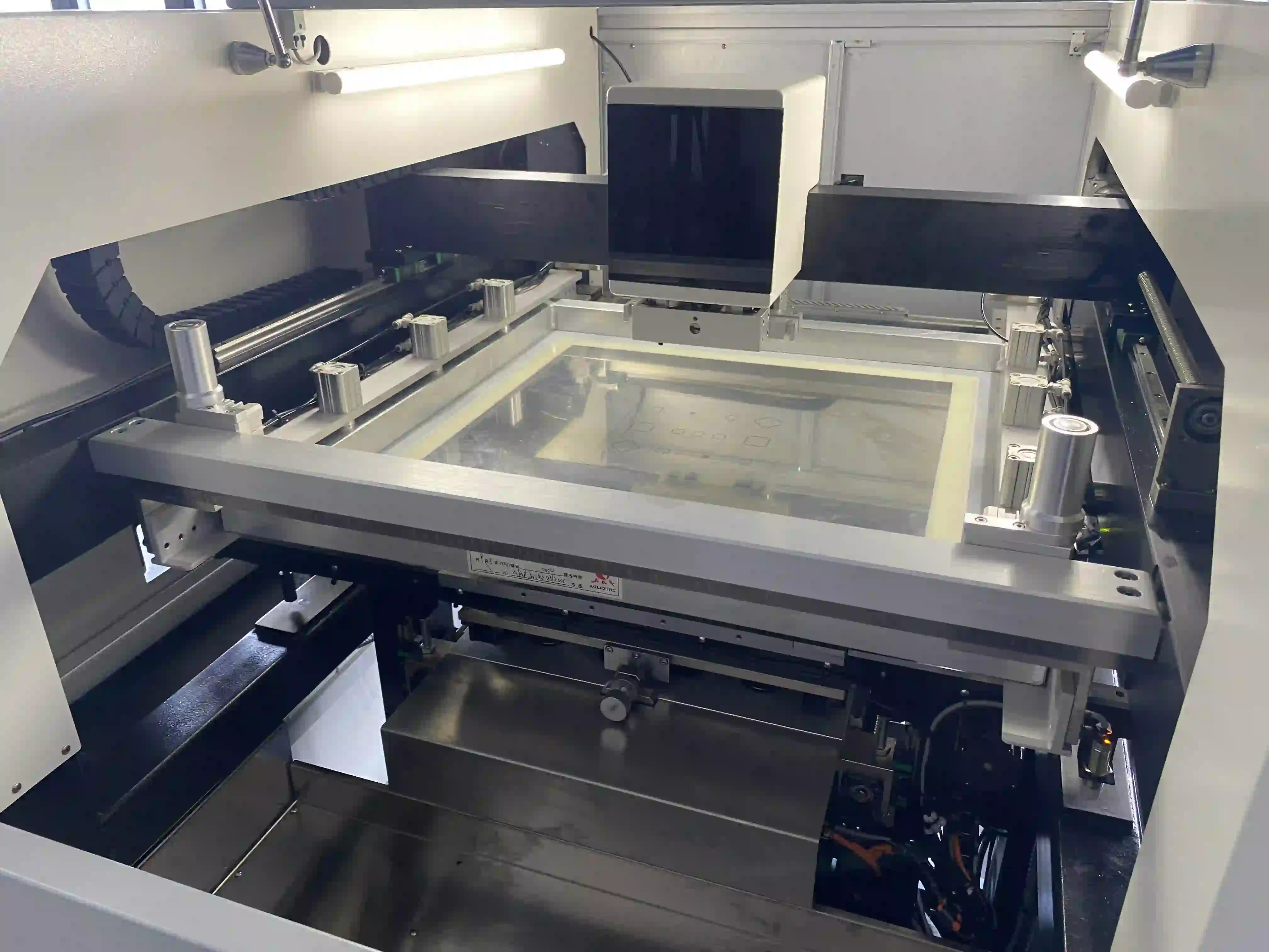
Stencil Printing
Stencil printing plays a crucial role in the PCB assembly process, serving as the foundational step for applying solder paste accurately onto circuit boards. This technique involves using a metal stencil with precise apertures to deposit solder paste onto the pads where components will be placed, ensuring reliable connections during reflow soldering. For engineers, hobbyists, and manufacturers searching for information on stencil printing, this tag gathers in-depth resources that address common challenges and optimize production workflows. Understanding the nuances of stencil design, such as aperture size, thickness, and material selection, can significantly reduce defects like bridging or insufficient paste volume, leading to higher yield rates in both prototype and high-volume runs. Practical applications of stencil printing extend from small-scale DIY projects to industrial SMT lines, where precision directly impacts the performance of electronic devices. Best practices include aligning the stencil properly with the PCB, maintaining consistent squeegee pressure, and inspecting for paste uniformity to avoid issues like tombstoning or solder balls. Users often seek guidance on selecting the right stencil type, whether laser-cut or chemically etched, and troubleshooting equipment like manual printers or automated systems. By mastering these elements, you can achieve finer pitch printing for advanced components, enhancing overall assembly efficiency. The articles under this stencil printing tag provide detailed insights into emerging trends, such as nano-coatings for improved release and software tools for stencil optimization. Whether you are refining your process for better repeatability or exploring cost-effective alternatives to traditional methods, these resources offer valuable knowledge to elevate your electronics projects. Readers can find step-by-step tutorials, case studies, and expert tips that align with real-world scenarios, helping to streamline your approach to PCB fabrication.
Technical Articles
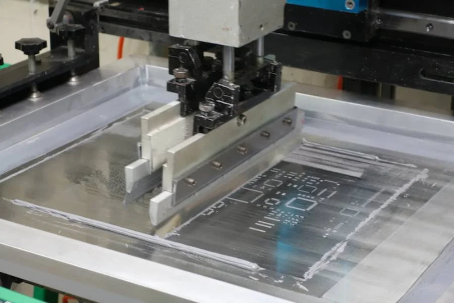
Why SMT Yield Often Stalls: Solder Paste Printing Controls That Directly Impact Quality
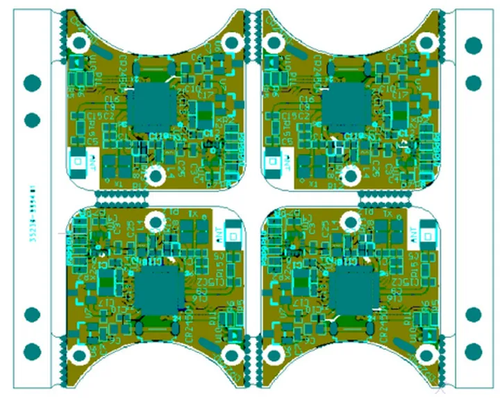
Why Adding Process Edges to a PCB Panel Is Not Wasted Board Material

Establishing a Precision Stencil Printing Process for Miniaturized Electronics Assembly

Preventing Solder Paste Printing Defects in SMT: Practical Process Control from Stencil to SPI
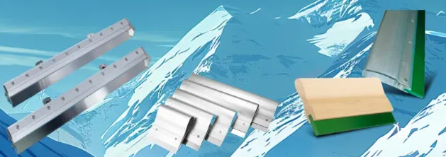
Mastering Squeegee Choices for Flawless Solder Paste Application in PCB Assembly
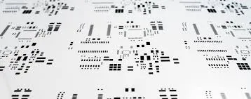
How Does Stencil Design Impact PCB Assembly Quality?
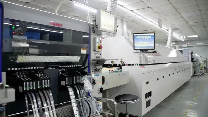
High Volume SMT Assembly: Best Practices for Reliable PCB Manufacturing
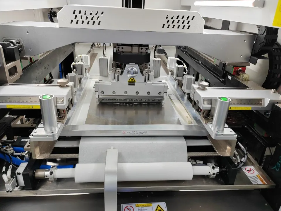
DIY Solder Paste Stencils: A Hobbyist's Guide to Low Cost PCB Assembly
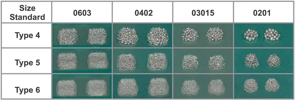
Stencils and Solder Paste: A Comprehensive Guide to Materials
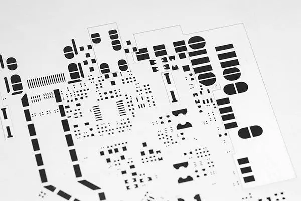
The Ultimate Guide to Surface Mount Stencils: From Design to Assembly
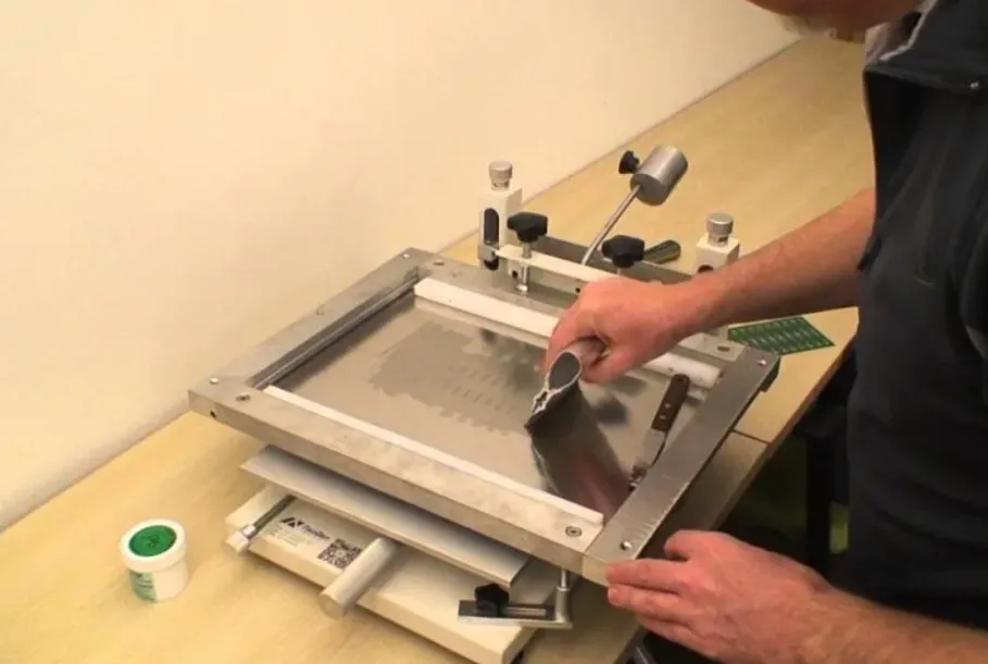
Step-by-Step Guide to Use a PCB Stencil
Solder Paste: Working With Fine Pitch Components and Their Application
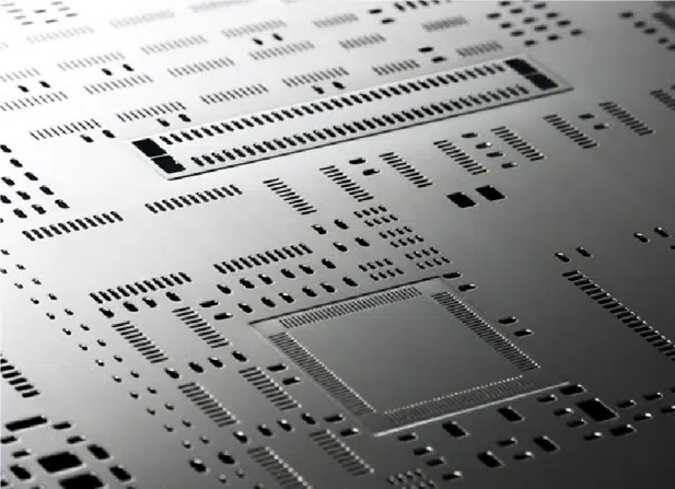
The Comprehensive Guide to SMT Stencil Engineering: From Design Optimization to Process Control
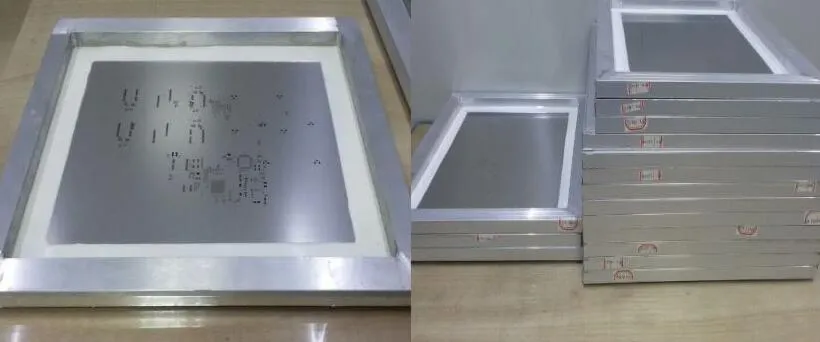
Step Up vs. Step Down Stencils: Understanding the Differences
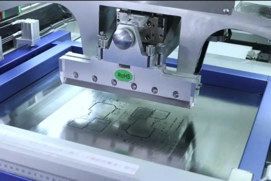
The Ultimate Guide to Stencil Printer Maintenance: Ensuring Consistent Solder Paste Deposition
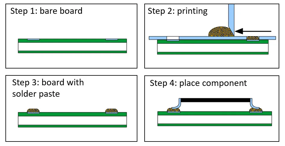
From Prototype to Production: Choosing the Right Stencil Printer for Your PCB Assembly Needs
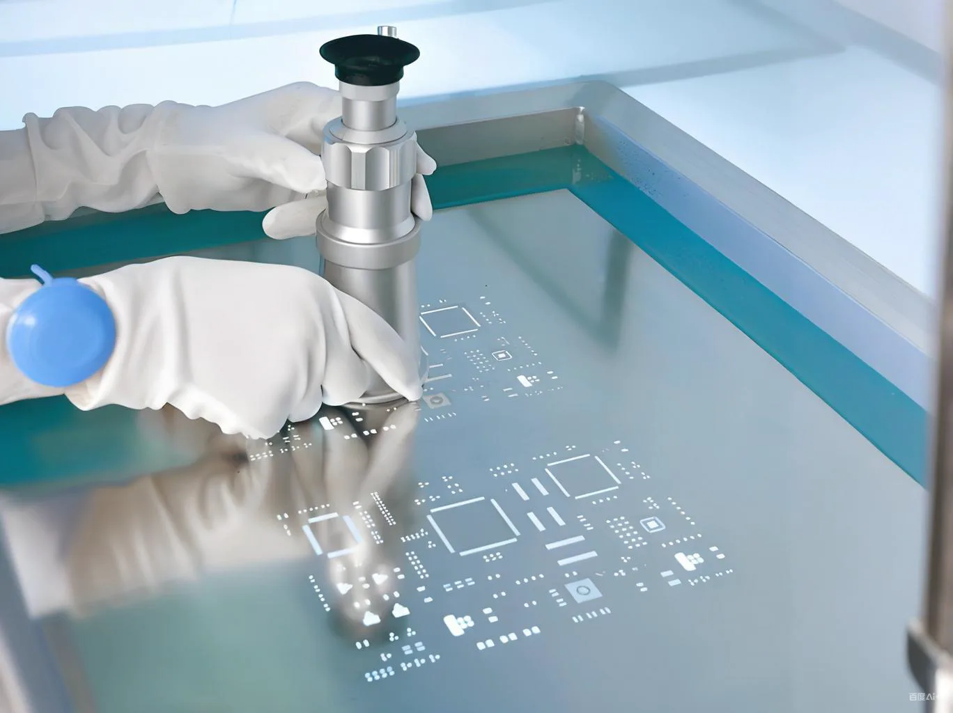
Precision Solder Paste Application: Mastering Stencil Printers for Fine Pitch PCBs
Advanced Stencil Printing Techniques: Achieving High Density SMT Assembly