02:50
02:50
Via Manufacturing
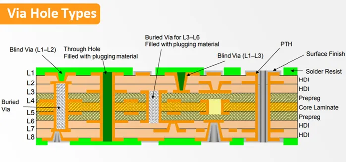
Vias play a crucial role in printed circuit board (PCB) design and production, serving as the essential conduits that enable electrical connections between multiple layers. In the realm of Via Manufacturing, this tag encompasses a comprehensive collection of resources focused on the processes, techniques, and challenges involved in creating these interconnections. Whether you are an electronics engineer optimizing high-density interconnects or a manufacturer seeking to enhance production efficiency, understanding via fabrication is key to ensuring signal integrity, thermal management, and overall board reliability. Delving into Via Manufacturing reveals practical applications such as selecting the appropriate via types—through-hole, blind, buried, or microvias—based on board complexity and performance requirements. Best practices include precise drilling methods like mechanical or laser drilling to minimize defects, followed by electroless and electrolytic plating for robust conductivity. Actionable insights from our articles address common pitfalls, such as via tenting to prevent solder bridging or implementing via-in-pad designs for space-constrained layouts. These strategies not only reduce manufacturing costs but also improve yield rates in high-volume production environments. For those troubleshooting issues like via cracking under thermal stress or aiming to comply with industry standards like IPC-6012, the content here offers detailed guidance on materials selection, such as using high-Tg laminates or advanced fillers for better durability. By exploring the articles linked under this tag, you can gain in-depth knowledge on innovative manufacturing tools and emerging trends, empowering you to refine your PCB projects with confidence and precision.
Video Guide
-
02:50
Technical Articles
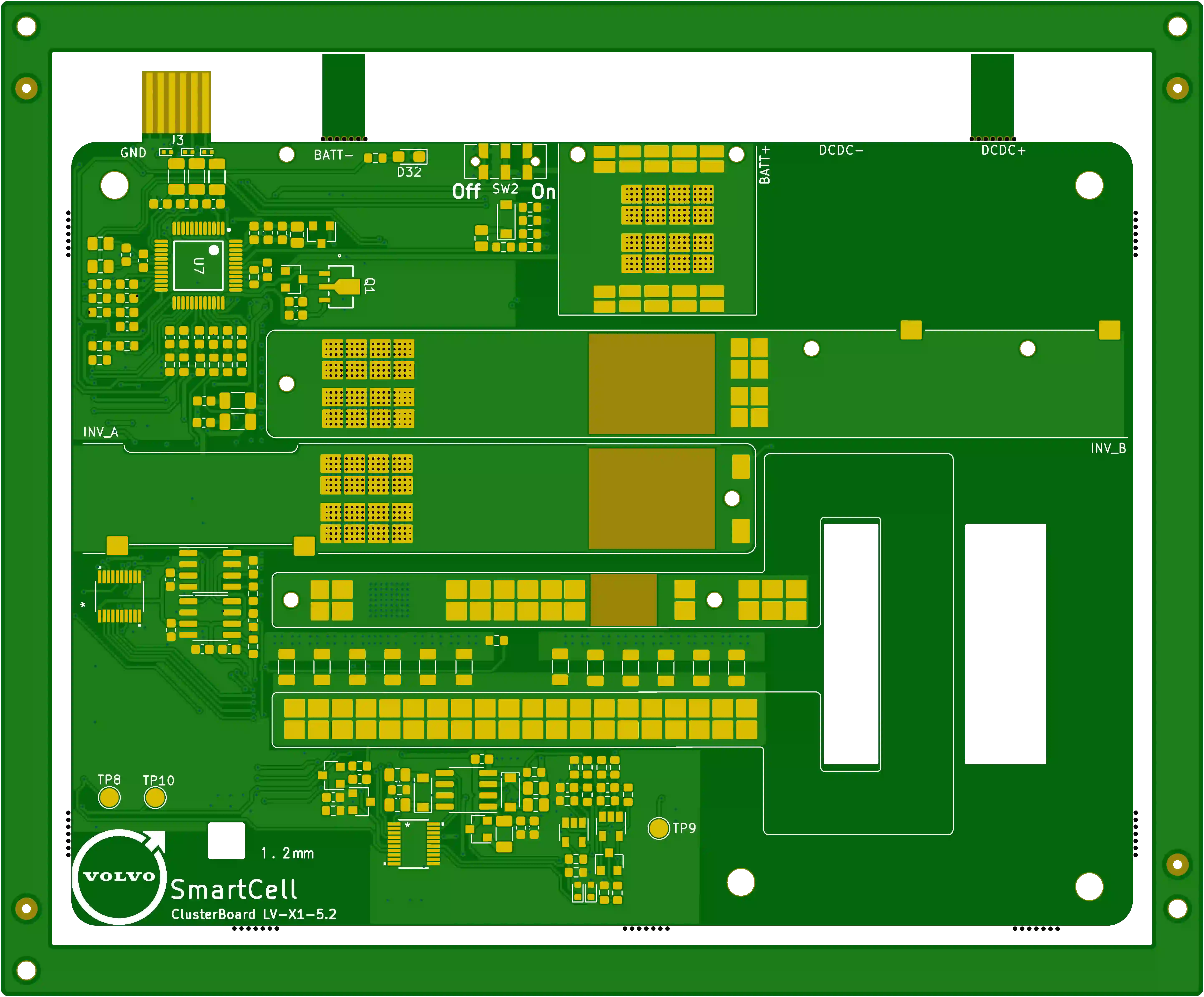
Evaluating 1.2mm Thickness Control and Depth Drill Precision in 4-Layer FR4 Production
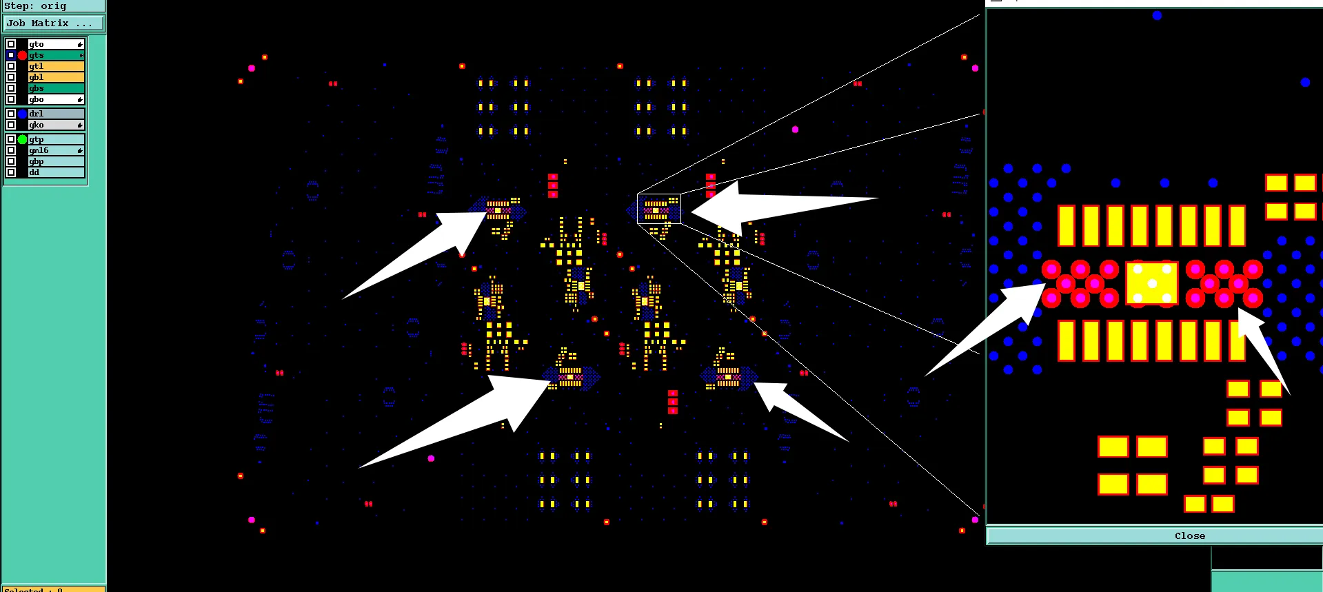
Resolving Tented Via vs Open Via Mismatches in PCB Manufacturing
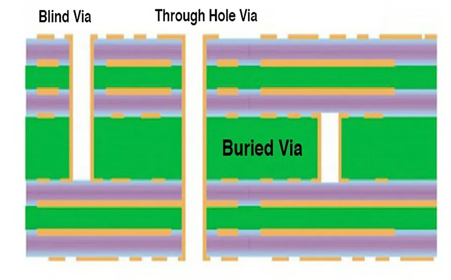
Blind Vias for Beginners: A Hobbyist's Introduction to Advanced PCB Design
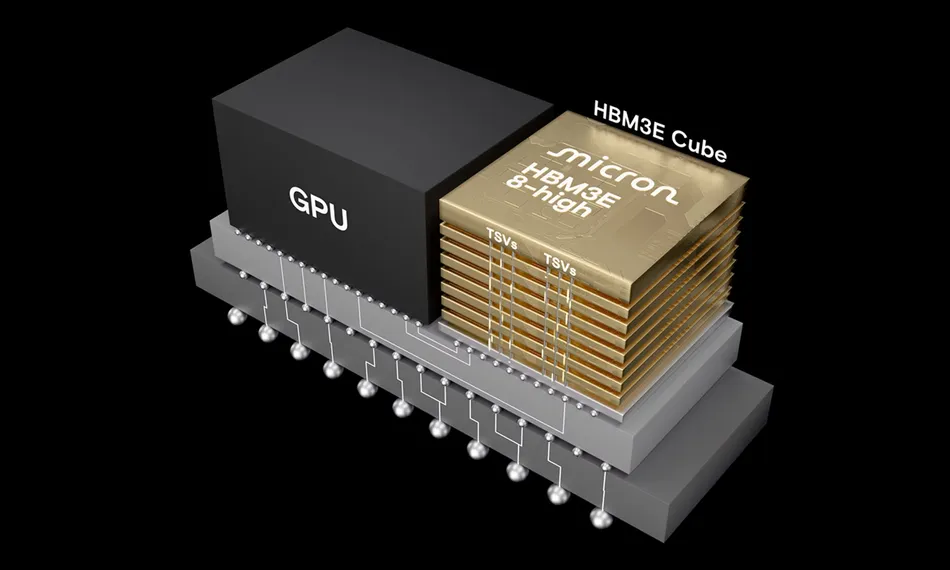
Comparing HBM, HBM2, HBM3 and HBM3e
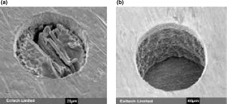
Optimizing Laser Drilling Parameters: A Deep Dive into Power, Frequency, and Speed
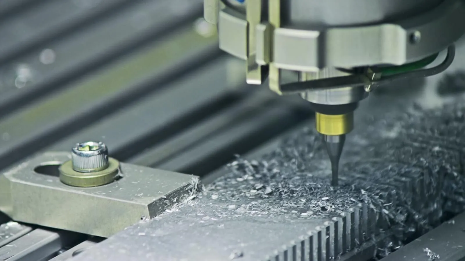
Laser vs. Mechanical Drilling: Which is Better for Your PCB Project?
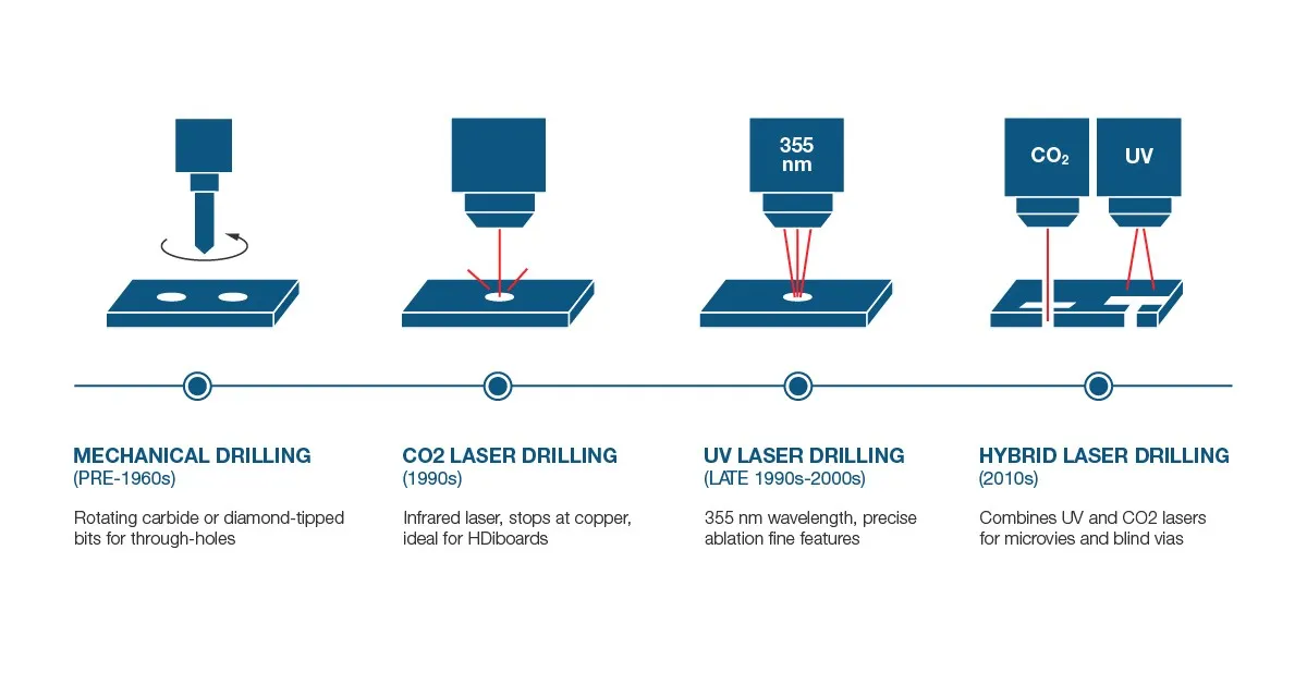
PCB Laser Drilling: How it Works, Benefits, and Applications
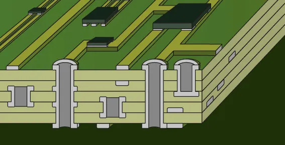
The Art of Layer Connection: Mastering Blind and Buried Vias in Multilayer PCBs