


PCB Manufacturing
Printed Circuit Boards (PCBs) form the backbone of modern electronics, serving as the essential platform where components connect to create functional devices. In the PCB Manufacturing category, readers gain access to a comprehensive collection of resources designed to demystify the intricate processes involved in producing these critical elements. From initial design considerations to final assembly and testing, this category covers every stage, providing valuable insights for engineers, hobbyists, and industry professionals alike. Understanding PCB manufacturing is crucial for anyone involved in electronics development. This field encompasses a wide range of topics, including material selection, such as FR-4 substrates and advanced laminates, as well as fabrication techniques like etching, drilling, and soldering. Articles here delve into best practices for optimizing layouts to minimize signal interference, ensuring reliability in high-stakes applications. Tutorials guide users through prototyping methods, while in-depth analyses explore emerging trends like flexible PCBs and additive manufacturing, which are revolutionizing industries from consumer gadgets to aerospace systems. The practical value of mastering PCB manufacturing extends to real-world scenarios, where efficient production can reduce costs, enhance performance, and accelerate time-to-market. For instance, insights on multilayer board construction help in designing compact devices for IoT applications, and discussions on quality control standards prevent common pitfalls in mass production. By engaging with the diverse guides and expert perspectives in this category, readers can build a solid foundation in PCB technologies, apply proven strategies to their projects, and stay ahead in an ever-evolving field. Whether troubleshooting assembly issues or exploring sustainable manufacturing practices, the knowledge shared here empowers informed decision-making and innovation in electronics.
Latest Blogs
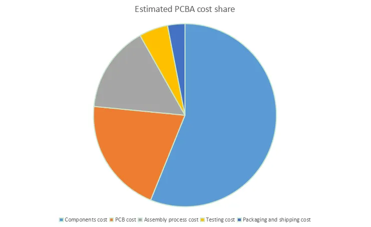
Cost Effective PCB Manufacturing: 10 Ways to Reduce Your PCB Costs Without Sacrificing Quality
Achieve cheap PCB manufacturing with 10 strategies that deliver pcb cost reduction in design, materials, and assembly. Lower pcb design cost, pcb materials cost, and enable low cost PCB assembly while preserving quality and reliability for electric engineers.
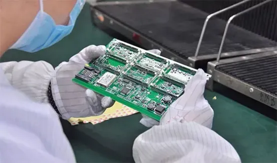
Top 7 PCB Testing Methods to Guarantee Quality and Reliability
Top 7 PCB testing methods including AOI, X-ray inspection, in-circuit testing, flying probe testing, and burn-in testing ensure board quality and reliability. Factory guide for electric engineers covers visual checks to functional tests for defect prevention.
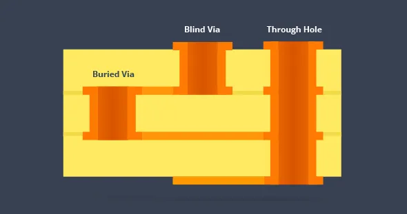
Via Technology in PCB Manufacturing: Types, Design Rules, and Optimization Techniques
Via technology in PCB manufacturing includes blind via PCB, buried via PCB, microvia design, via in pad, and thermal via placement. This article covers types, essential design rules per IPC standards, and practical optimization techniques for reliable high-density multilayer boards and better yields.
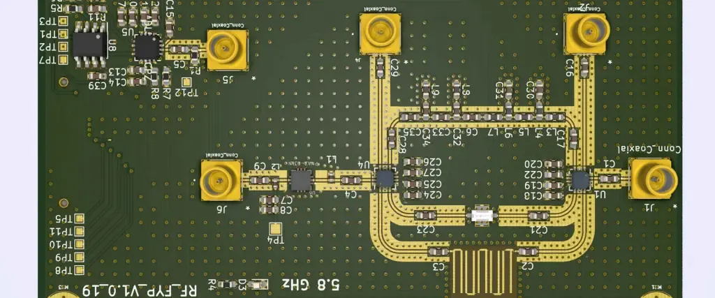
5G PCBs: Designing for High Frequency Performance and Signal Integrity
Discover how to design 5G PCBs for superior high-frequency performance and rock-solid signal integrity. This guide covers low-loss materials, precise impedance control, optimized stack-ups, thermal management, and manufacturing best practices for mmWave applications.
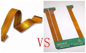
Bend, Don't Break: The Rise of Flexible and Rigid Flex PCBs in Modern Electronics
Flexible PCB design guidelines ensure reliability in dynamic applications. Details cover rigid flex PCB manufacturing process, polyimide PCB substrate properties, dynamic bending PCB techniques, and flexible PCB applications in wearables automotive and medical devices for electric engineers.
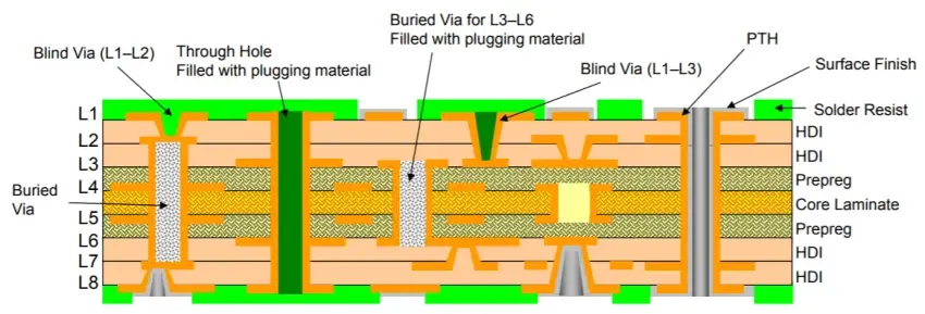
Miniaturized HDI PCB: Design and Manufacturing for Small Form Factor Electronics
Explore miniaturized HDI PCB design and manufacturing for small form factor electronics. Learn how microvias, HDI stack-ups, sequential lamination, and fine-line routing enable compact, high-density PCB solutions without compromising reliability and signal integrity.
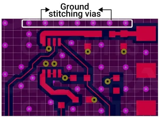
PCB Design for Signal Integrity: Techniques for Minimizing Noise and Interference
Master PCB signal integrity with proven techniques for minimizing noise, interference, crosstalk, and reflections in high-speed designs. Learn grounding, shielding, stackup, and routing strategies that deliver reliable performance and faster time-to-market for engineers.
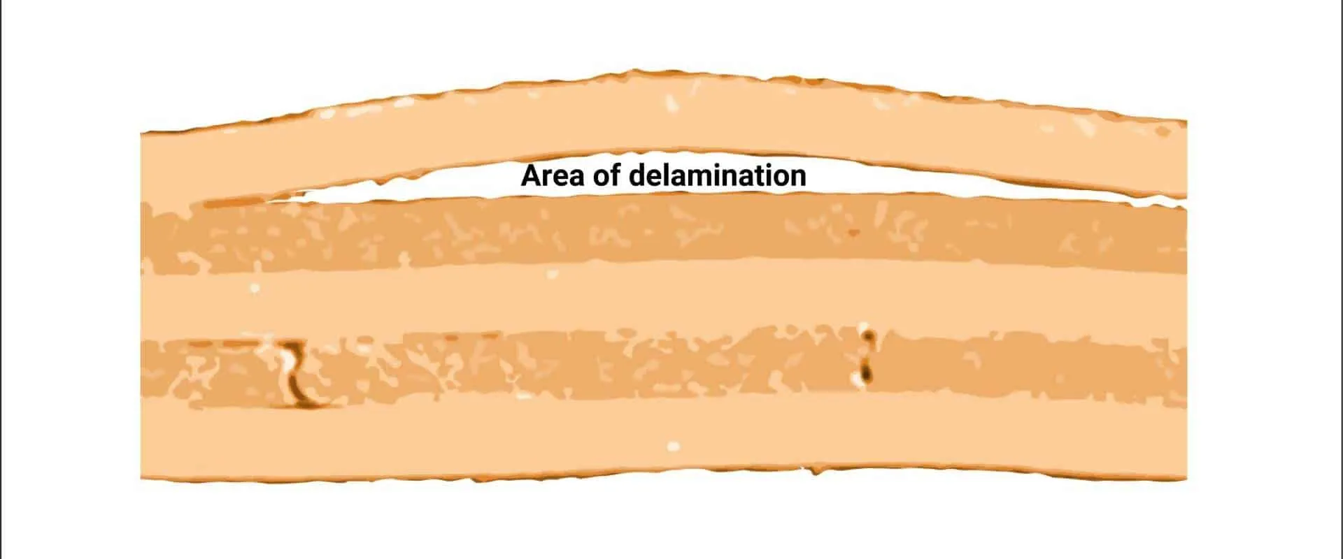
Overcoming PCB Manufacturing Challenges: Solutions for Common Defects and Production Issues
Address PCB manufacturing defects like delamination, warpage, plating voids, and hole issues with practical solutions and best practices. This guide covers causes, prevention strategies, and IPC standards to resolve production problems and improve yields for electric engineers.

In Circuit Testing with Dual Site Test
Dual site in circuit testing enables parallel testing of two PCBs in one fixture, driving scalability through multi site architecture. Maintain accuracy and reliability in quality control while reducing costs for high volume production. Electric engineers get technical principles, best practices, troubleshooting, and FAQs.

Different In Circuit Testing for Complete Defects Coverage
Compare bed of nails testers and flying probe testers for in circuit testing that delivers complete defects coverage. Match approach and application suitability to specific production needs regarding volume scale and design complexity to boost PCB assembly quality and yield for electric engineers.
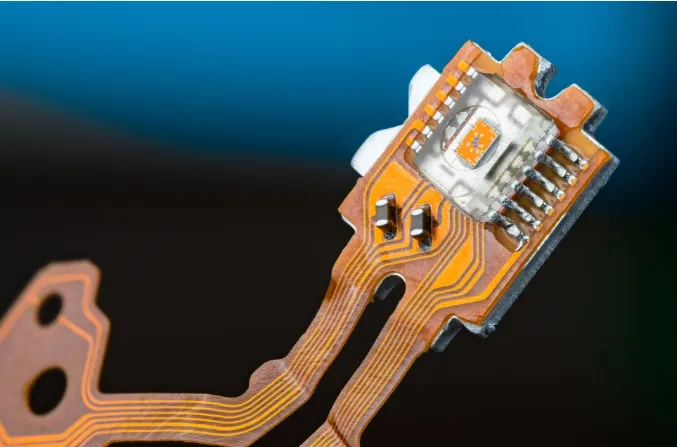
Plasma Etching for Flexible PCBs: Gentle Etching for Delicate Substrates
Plasma etching delivers gentle low temperature processing for flexible PCB etching on delicate substrates. It ensures precision anisotropy and cleanliness without warpage. Details include technical principles advantages best practices troubleshooting and standards for reliable flexible electronics production.
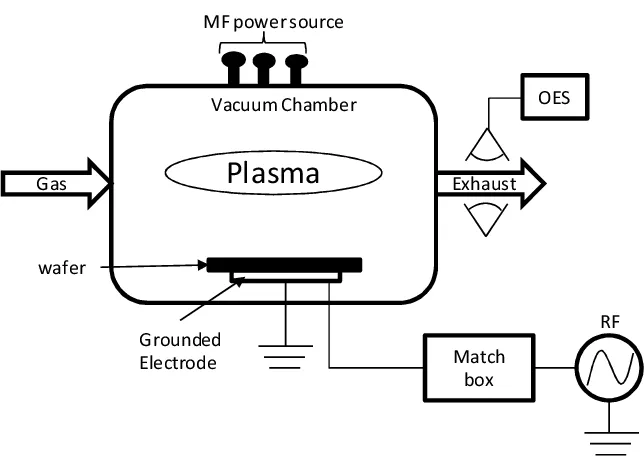
The Environmental Benefits of Plasma Etching in PCB Manufacturing: A Sustainable Approach
Plasma etching brings clear environmental gains to PCB manufacturing by cutting hazardous waste, skipping chemicals, and saving water. This approach fits sustainable PCB needs with precise desmear, lower emissions, and easier compliance for green production lines.


