PCB Etching
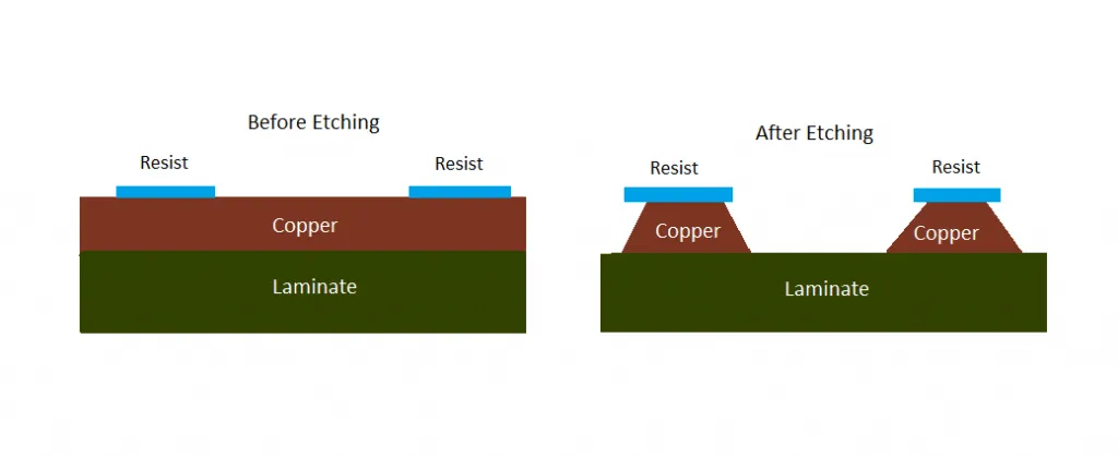
PCB etching is a fundamental process in electronics manufacturing and prototyping, allowing enthusiasts, engineers, and hobbyists to create custom printed circuit boards by selectively removing copper from a substrate to form conductive traces. This technique is essential for anyone looking to transition from breadboard designs to more permanent and reliable circuits, whether for personal projects, educational purposes, or small-scale production. By understanding PCB etching, users can achieve precise control over board layouts, reducing errors and improving signal integrity in their electronic devices. The process typically involves applying a resist material to protect desired copper areas, followed by exposure to an etchant solution such as ferric chloride or ammonium persulfate, which dissolves the unprotected metal. For those new to the field, starting with photoresist methods offers high accuracy, while toner transfer techniques provide a cost-effective entry point using everyday laser printers. Key best practices include working in a well-ventilated area to handle chemicals safely, wearing protective gear to avoid skin contact, and properly disposing of waste to minimize environmental impact. Advanced users might explore double-sided etching or incorporating vias for complex multilayer designs, which can significantly enhance functionality in applications like IoT devices or custom sensors. Articles tagged under PCB Etching on this site delve into step-by-step tutorials, troubleshooting common issues like under-etching or over-etching, and comparisons of etching kits versus professional services. These resources equip readers with practical knowledge to optimize their workflows, from selecting the right etchant to integrating etching with soldering and assembly. For deeper insights into related topics such as PCB design software or alternative fabrication methods, browsing connected tags can further support your electronics journey.
Technical Articles
Step by Step: Creating Inner Layers Using Home Etching Methods
Demystifying Copper Foil Thickness: A Beginner's Guide for PCB Hobbyists
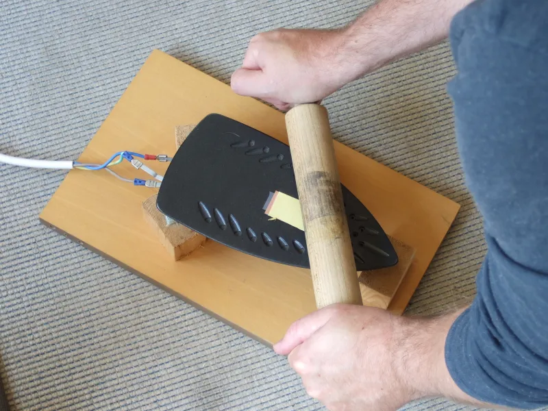
DIY PCB Solder Masking: A Beginner's Guide to Protecting Your Homebrew Boards
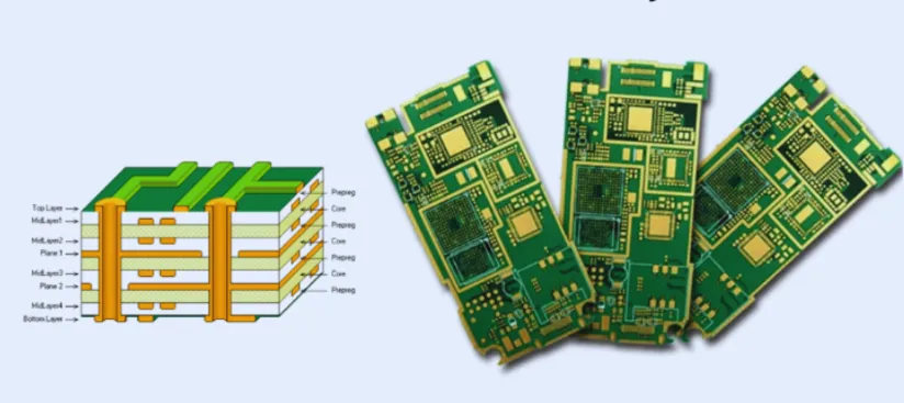
Crafting Multi-Layer PCBs at Home: A Hobbyist’s Guide to Advanced Board Fabrication
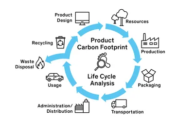
Comprehensive PCB Life Cycle Assessment: A Guide to Sustainable Electronics
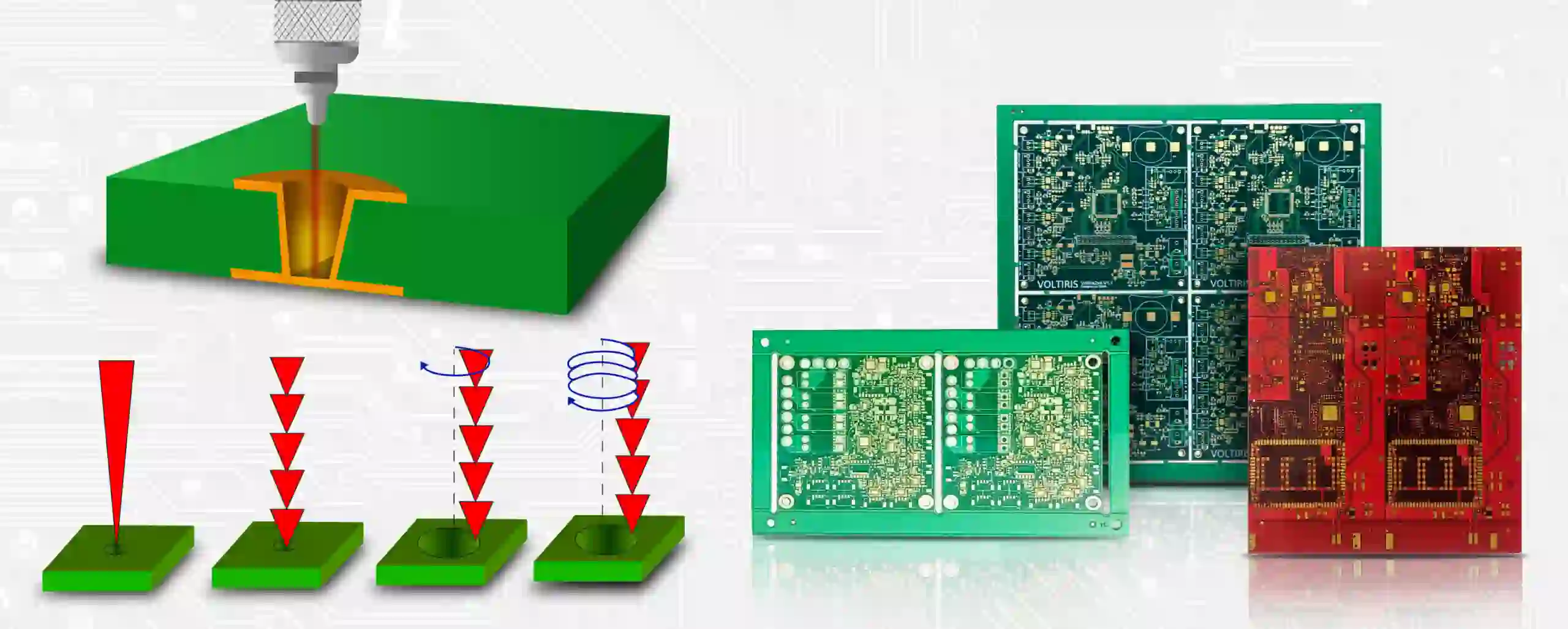
Manufacturing Heavy Copper PCBs: A Step by Step Guide
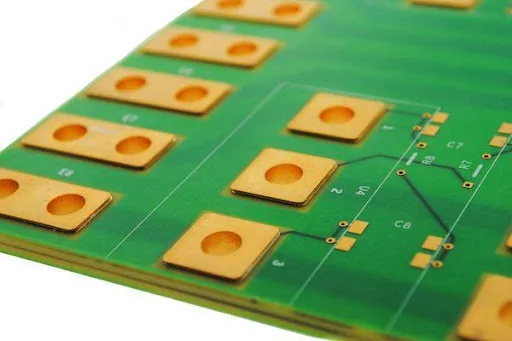
Manufacturing Challenges and Solutions for 3 oz Copper PCBs
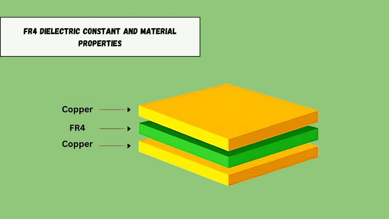
Demystifying FR 4 Manufacturing: A Step by Step Guide
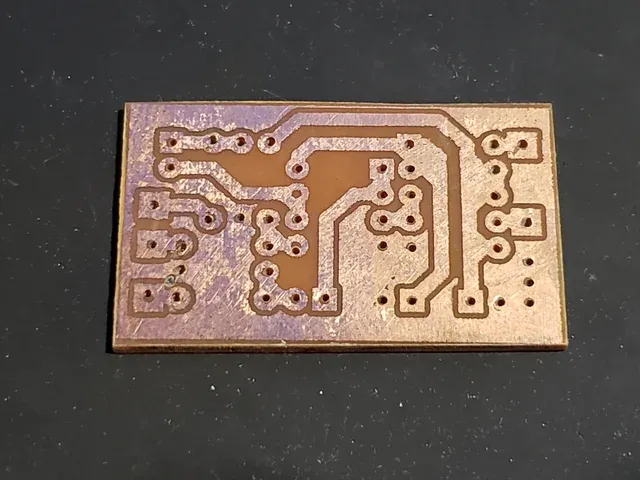
DIY PCB Etching at Home: A Safe Guide Using Vinegar and Peroxide
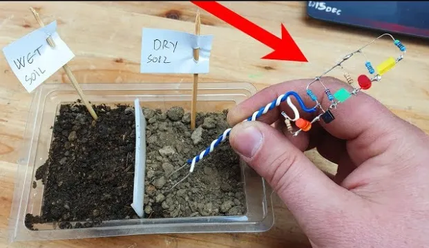
Build a DIY Soil Moisture Sensor: Custom PCB & Arduino Guide
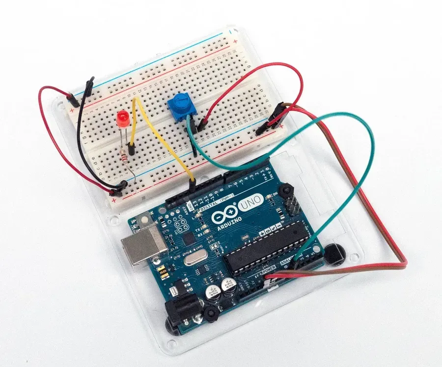
Build Your Own Heart Rate Monitor: A Beginner's Custom PCB Guide
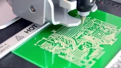
Understanding Trace Width Tolerances in PCB Manufacturing for Reliable Designs
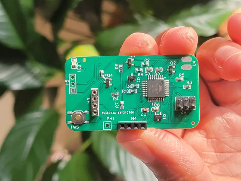
Recyclable PCB Materials: A Guide for Hobbyists
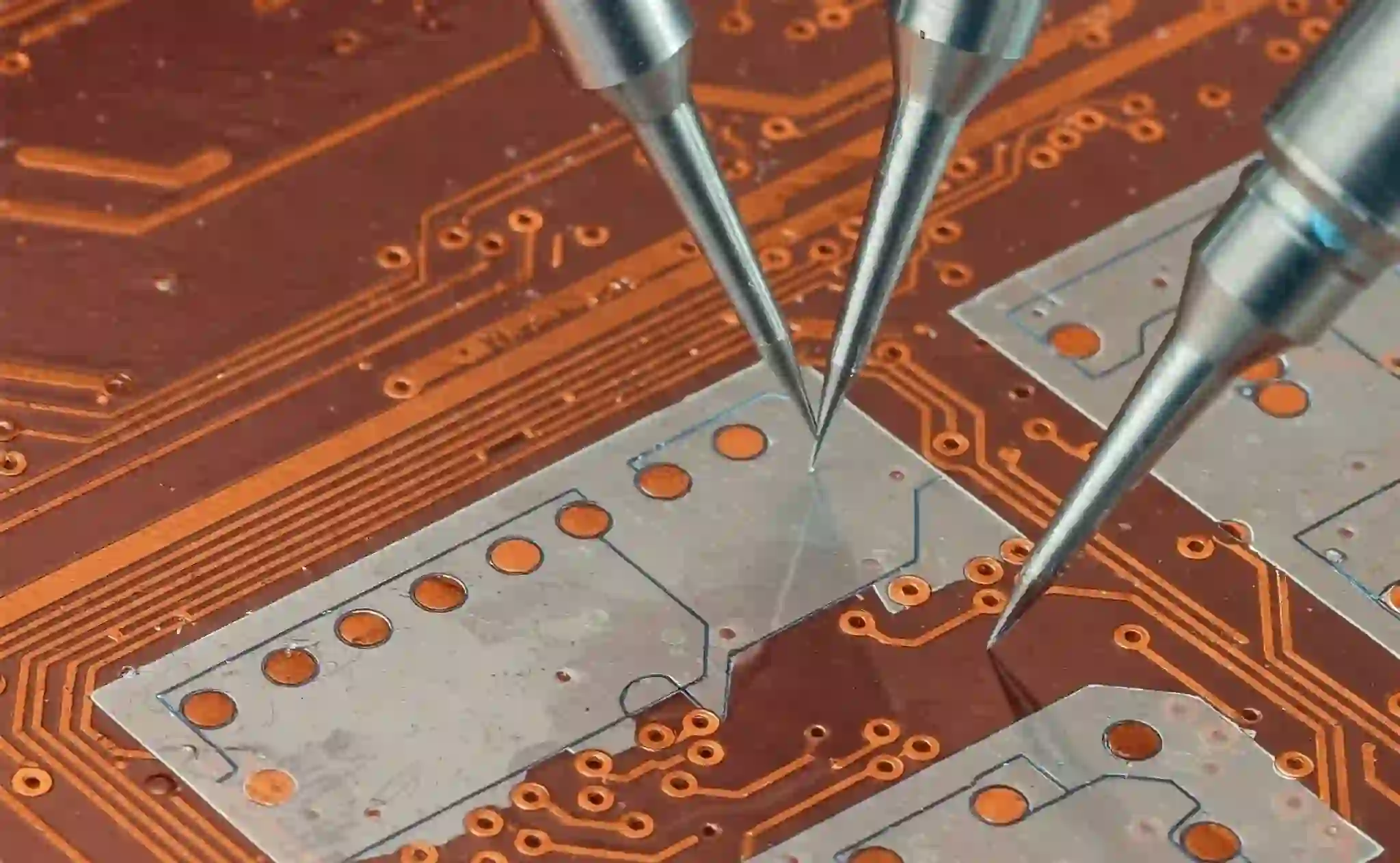
Troubleshooting PCB Etching Problems: Undercutting, Over-Etching, and Uneven Etching
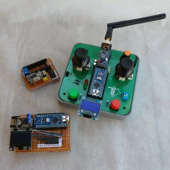
Building a Simple Radio Receiver with a Single-Layer PCB
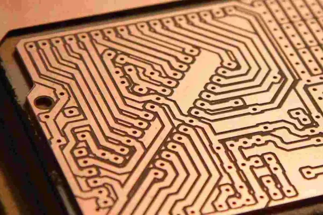
PCB Prototype Manufacturing for Beginners: A Hobbyist's Guide
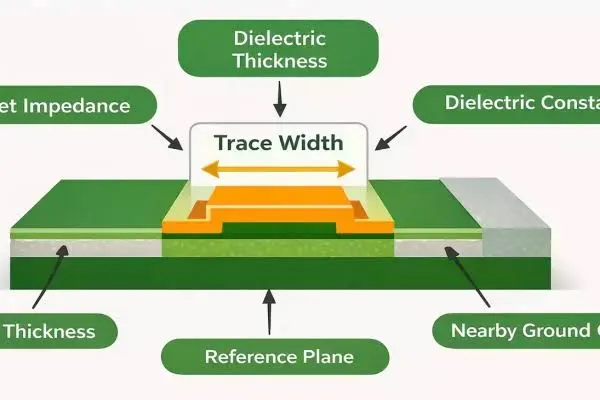
FR4 PCB Minimum Trace Width: What Designers Should Know
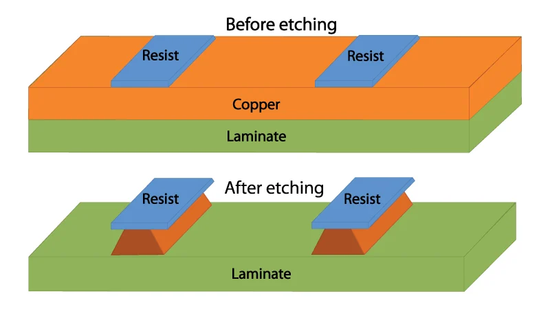
FR4 PCB Etching Undercut: Causes and Process Control