 03:18
03:18
PCB Warpage
PCB warpage refers to the undesirable bending or deformation of printed circuit boards during manufacturing, assembly, or operation, often caused by thermal expansion mismatches, uneven material distribution, or mechanical stresses. This phenomenon can lead to significant challenges in electronics production, such as misalignment of components, solder joint failures, and reduced reliability in high-density assemblies. For engineers, designers, and manufacturers searching for information on PCB warpage, understanding its root causes is essential to mitigate risks and ensure product quality. Common triggers include asymmetric copper layering, improper lamination processes, or exposure to extreme temperatures during reflow soldering, which can result in boards that fail to meet flatness specifications like those outlined in IPC standards. Addressing PCB warpage effectively involves a combination of design strategies and fabrication techniques. For instance, optimizing layer stackups to balance copper densities on both sides of the board can minimize thermal imbalances, while selecting materials with compatible coefficients of thermal expansion (CTE) helps prevent deformation under heat. Practical best practices include conducting finite element analysis (FEA) simulations early in the design phase to predict potential warpage and incorporating features like stiffeners or controlled cooling rates during production. In high-stakes applications such as automotive or aerospace electronics, where reliability is paramount, these measures not only reduce defects but also enhance yield rates and long-term performance. Professionals dealing with PCB warpage will find valuable resources in the articles tagged here, offering detailed case studies, measurement methods using tools like shadow moiré or laser profilometry, and step-by-step guides to corrective actions. By delving into these topics, readers can apply proven solutions to their own projects, from prototyping to mass production, ultimately improving efficiency and reducing costly rework.
Video Guide
-
03:18
Technical Articles
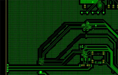
HDI PCB Copper Balance: Why Uneven Copper Distribution Matters
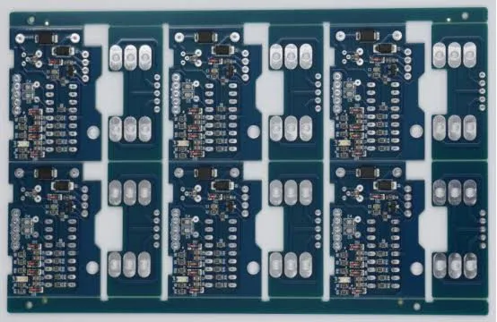
How to Prevent Solder Bridging on Fine-Pitch HDI BGA Pads
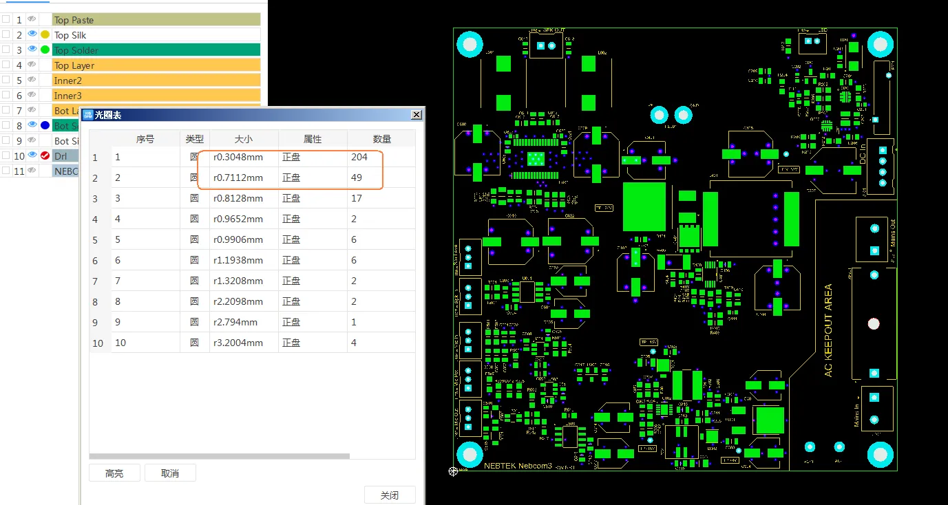
How DFM Prevented Via Tenting Issues in 4-Layer FR4 PCB
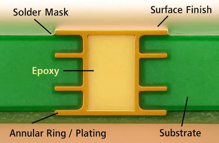
How to Avoid Solder Mask Issues Around HDI Microvias
Designing PCB Stackups in KiCad for Manufacturing: Layer Planning Guide
Preventing Exposed Copper from Copper to Outline Clearance Issues

Common FPC Manufacturing Defects and How to Prevent Them
Why Do FPC Boards Shrink After Lamination?
Sheet Metal Fabrication Process Explained: From Design to Finished Parts
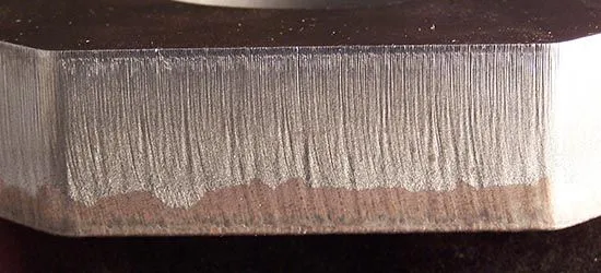
How Laser Cutting Quality Is Controlled in Sheet Metal Fabrication
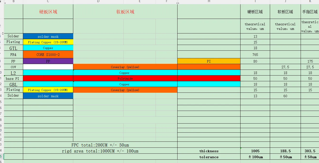
Rigid-Flex PCB Stackup Design: Balancing for Warpage Control
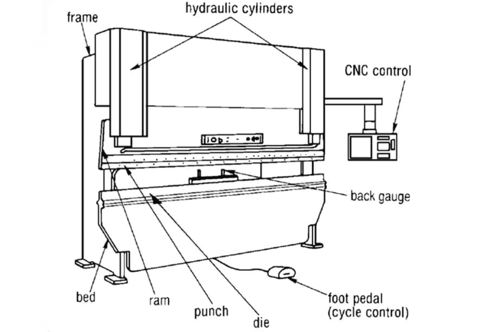
How Sheet Metal Bending Accuracy Is Controlled: Factors and Best Practices
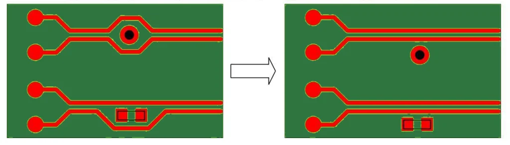
Mastering Metal Core PCB Routing: Tips and Tricks for Optimal Performance
Rigid PCB Failure Analysis: Identifying Root Causes and Preventing Future Issues
Finding the Right PTFE PCB Supplier: Key Considerations for Quality and Cost
How to Choose the Right Thickness for Your Metal Core PCB
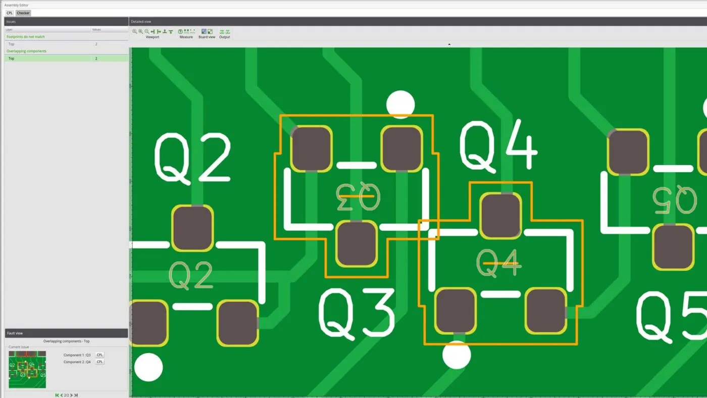
The Importance of Courtyard Areas: Preventing Assembly Mishaps in PCB Design
Hatched vs. Solid Copper Pour: Choosing the Right Approach for Your PCB Design
The Art of Lamination: Achieving Perfect Layer Bonding in Multilayer PCBs