When a panel is released with stamp holes (mouse-bite holes) on a breakaway tab, the question that usually reaches CAM is not "what pitch should this row use." It is whether the hits already in the drill still leave a connecting tab after the outline is routed, whether that tab is supposed to stay intact through the rest of the process, and whether the break will come off clean or leave a proud edge.
The rest of this article stays on that row: how far the holes sit from each other, how much laminate remains between them, and where the row sits on the board outline. Rail width, array efficiency, and V-score belong to other reviews.
| Released finding | What is actually in front of CAM | What the factory usually proposes |
|---|---|---|
| Spacing too small to form a link | After drill, the laminate between adjacent holes is no longer a usable connecting tab | Delete one stamp hole on that tab; leave the outline alone |
| Spacing too small; the panel breaks easily | A tab is still there, but the remaining web or the routed tab looks too weak for handling | Leave the row as released, or change hole count or tab location after the customer replies |
| "Bridge" position too small, add position wrong, too many burrs; optimized sketch attached | The hits sit where the break leaves a stub, lands on copper, or tears at a corner | Use the attached relocated row as production geometry |
All three findings start from a row that already exists. Who put that row there has to be clear before any of those proposals can close.
PCB Stamp Hole Design: Which File Defines the Row?
The same tab can arrive from more than one place in the package, and those places do not always tell the same story.
Sometimes the customer panel drawing already dimensions the stamp-hole row on each breakaway tab as part of real PCB panelization. Sometimes there is no panel drawing, and the board outline plus the NC drill are what actually place the hits. Sometimes the order note only says "stamp holes," "mouse bites," or "factory panelize." And sometimes the row shows up for the first time on a factory working-panel sketch after CAM has already looked at the files.
A note that names stamp-hole singulation tells the factory how the boards should come apart. It does not put holes on the tab. Count, tool, and location still have to come from the drill against the outline. If the unit Gerber never contained the row and the factory added it while building the working panel, that added row is still something to confirm the moment spacing or position will change. Until the customer accepts the sketch, it is a proposal, not the released design.
The same edge often carries other holes that look similar at a glance: a PTH or component hole, a tooling hole on the process edge, a plated slot used as an outline feature. Those are not the perforation. V-score language in the same note is a different singulation method and does not stand in for this row.
So the first pass is simply to line up the order or fabrication note, the customer panel drawing, the board outline, and the drill tool list at the tab, and say which of those sources defined hole count, hole tool, and row location. If only the factory sketch added the row, the EQ says so.
PCB Stamp Holes Spacing: What CAM Measures at the Breakaway Tab
Once ownership is stated, the useful picture is the stamp-hole hits laid on the board outline and on the routed channel that leaves the breakaway tab. That overlay answers a geometry question. It does not calculate whether the panel is "strong enough."
| What the overlay can show | What it cannot settle |
|---|---|
| Center distance from hole to hole along the row | Whether the panel will survive SMT handling |
| Laminate left between adjacent hole walls (the remaining web) | How much burr is acceptable after a hand break |
| How much of each hit sits on, inside, or outside the outline | Whether the designer wanted an easy snap or a stiff tab |
| Whether the row sits in the middle of the tab or is biased onto the unit | A factory-default pitch or a published mouse-bite dimension |
| Copper or silk that sits in the break path | Force, board thickness, or an acceptance limit |
"Spacing too small" gets used for more than one defect, and that is usually because three different lengths are being treated as one number. The center distance between hits is one length. The remaining web between hole walls is another. The tab width left by routing — unit outline to rail — is a third. A wide-spaced row on a very short tab can still break. A tight row on a wider tab can fail in a different way: there is nothing left to call a connecting tab.
Copper under or beside a hit shows up on the same overlay and will affect how the edge breaks. Seeing that copper is useful. Turning it into a clearance rule is not what this overlay is for.
Under that picture sit the drill tool, the outline, the routed gap, outer copper at the tab, and any dimension the customer already put on the panel drawing. Stamp holes stay NPTH unless that released tool is plated. Measuring those layers does not turn any of them into a limit.
Stamp-Hole Spacing That Leaves No Connecting Tab
The first EQ is blunt about the mouse bites clearance: after the holes are drilled, there is no connecting tab left that the factory is willing to run. The wording is that spacing is too small to form a link, and the factory will delete one stamp hole.
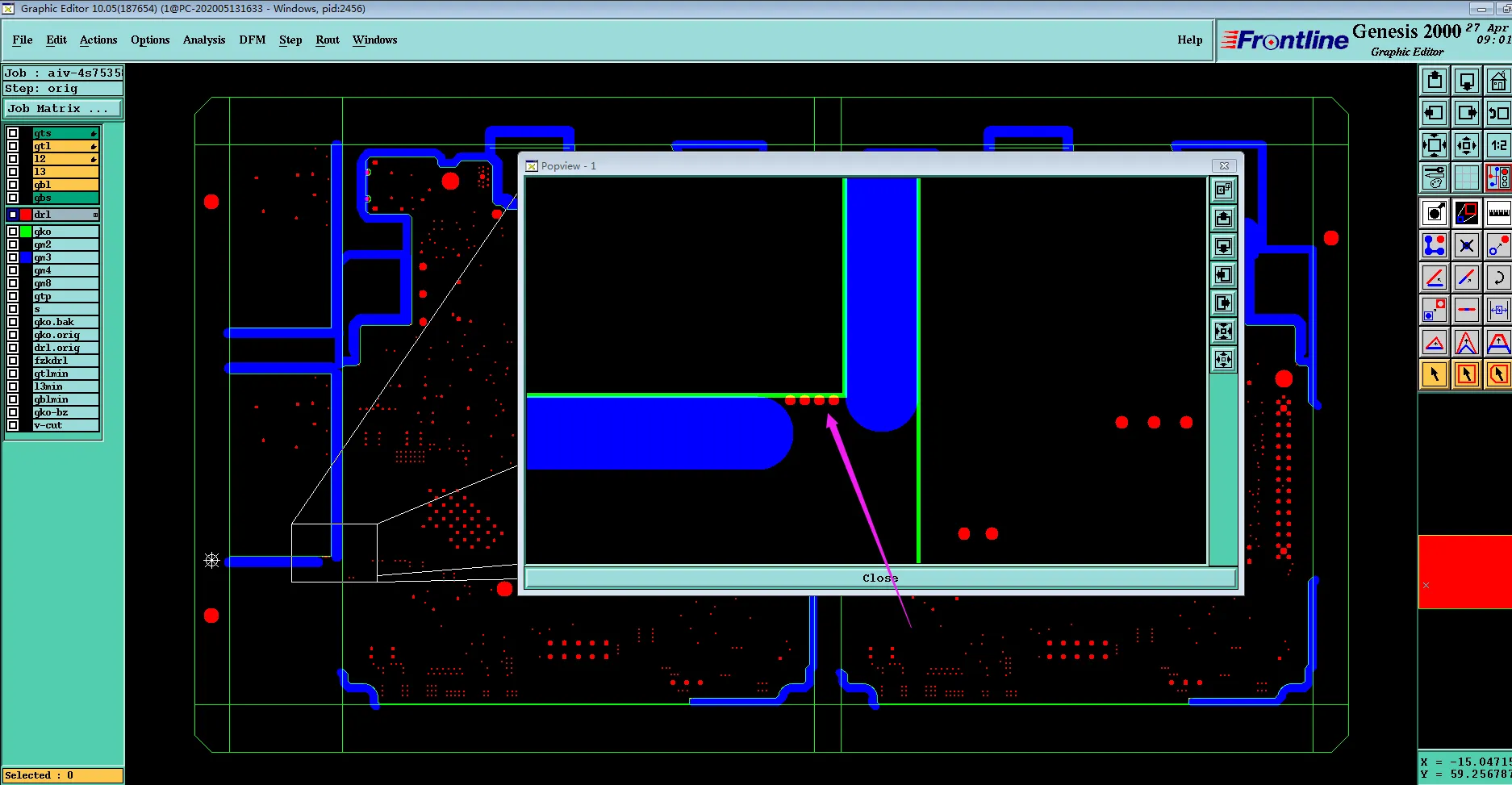
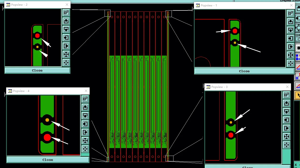
The PCB stamp holes spacing is too small.
Taking one hit out of the row leaves more laminate between the holes that remain. The board outline does not move. No V-score is added. The hole count on that tab is still part of what was released, even if the note only said "mouse bites," so the missing hit is not something CAM can assume the designer will accept.
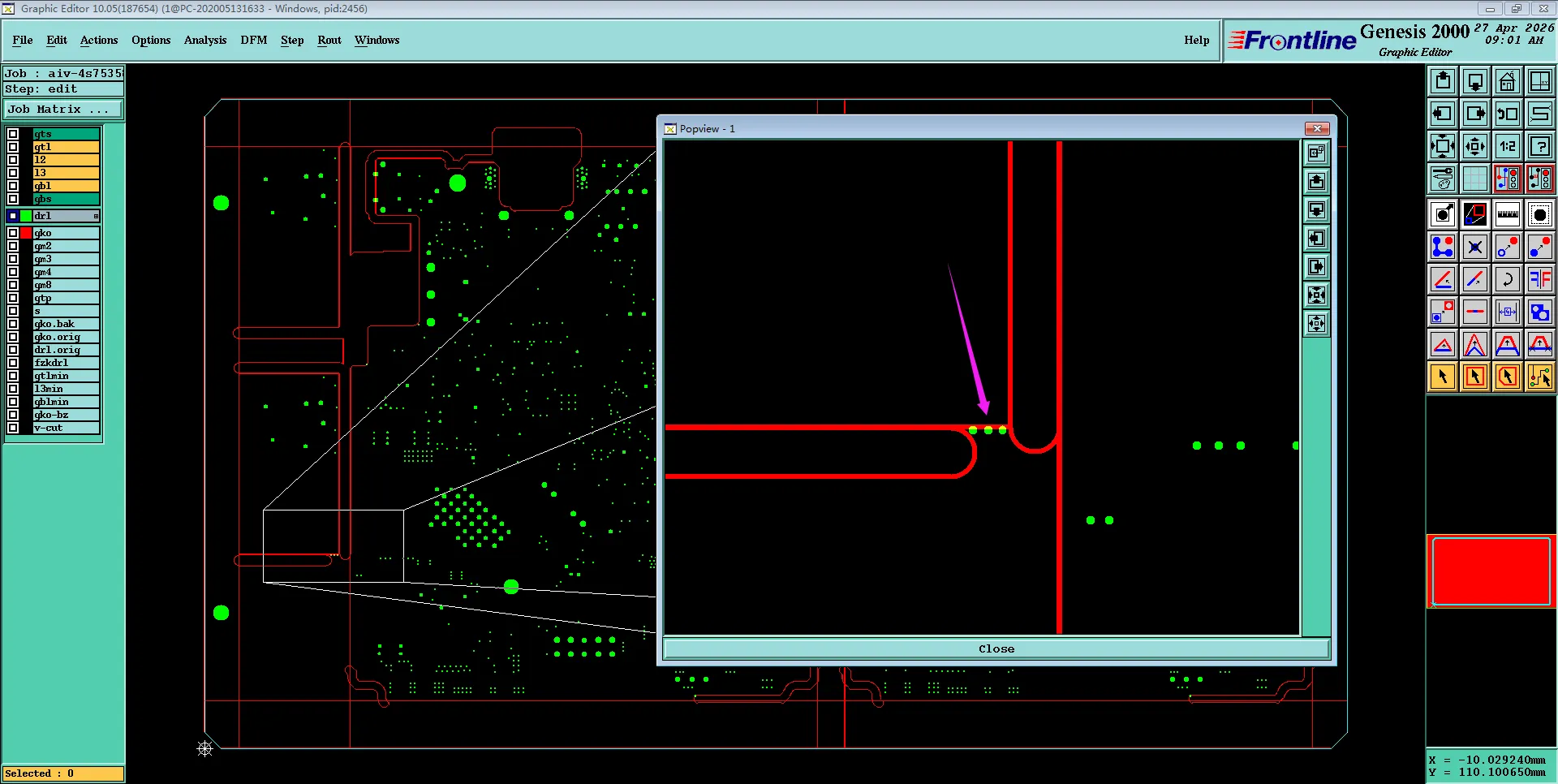
The factory will delete one stamp hole.
Leave the row as drawn and the web can tear in routing, in handling, or at the first break. The unit then comes off the rail at a place the drawing still showed as a tab.
What gets compared is straightforward: the released drill versus the proposed drill on that named tab — how many stamp-hole hits were there, and how much web sits between adjacent walls before and after the deleted hit. The hole being removed has to be a stamp hole, not a nearby PTH and not a tooling hole on the process edge. The customer either accepts the reduced count on that tab or keeps the released row. That is the whole close. It is not a request to redraw the pattern to a standard pitch.
PCB Stamp Hole Connection: When the Tab Is Too Weak for Handling
The second finding starts from a different place in the PCB stamp hole design. A tab is still there. The question is whether that tab is supposed to survive fabrication and assembly, or whether an early break is acceptable.
If the row lets go too soon, a unit drops off the rail, the array shifts in the conveyor or fixture, and copper near the tab can crack. When the customer writes that the "bridge" position is too small, they are often talking about where the tab sits and how much of it routing left, not only about hole-to-hole pitch.
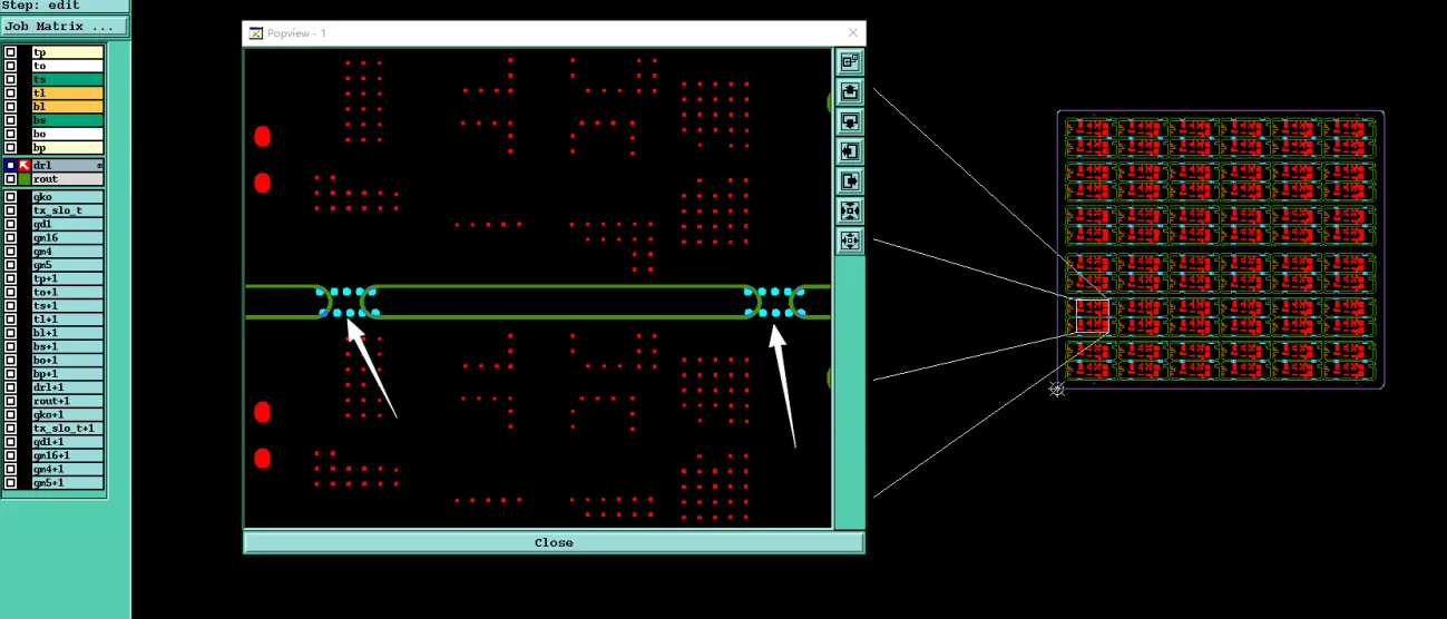
The stamp hole's spacing is too small, which can be easily lead to board broken.
The Gerber will not say whether these boards are meant to be snapped by hand at incoming or held in panel through SMT. That intent lives in the note, on the panel drawing, or in the reply to the EQ. Widening the tab or adding holes to stiffen the panel would be a different change, and it is not something the factory should do unmarked.
Here the overlay is read against the handling path the package already implies — the customer's own array, or the factory working panel. Copper, a component, or a connector on the break path is worth recording as present or absent. From there the customer either accepts the breakage risk as released or asks for a change to hole count, tab location, or singulation method. Nothing in the files gives CAM a force, a thickness, or a web-width number that would let that change be made alone.
PCB Stamp Hole Clearance and Burrs: Position on the Board Outline
Burrs after stamp-hole singulation have as much to do with where the hits sit on the finished outline as with how close the holes are to each other.
A hit that lives entirely outside the outline tends to leave a proud stub on the unit. A hit that sits on the outline tends to break closer to the intended edge. That is what the overlay shows. It is not a factory rule that every hole must be tangent to the outline.
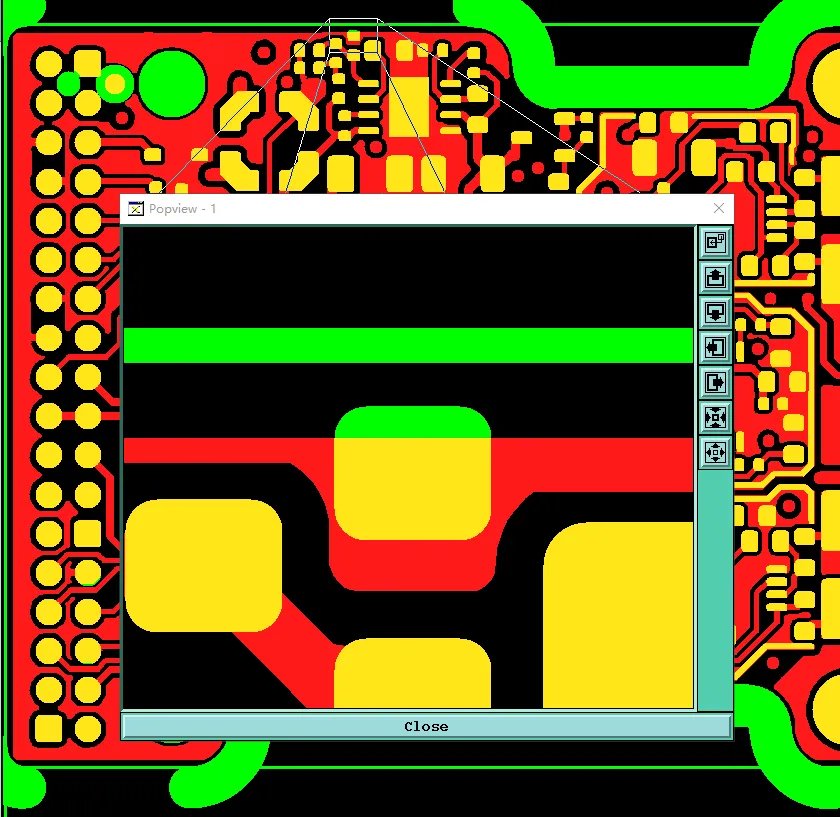
"Stamp hole added position is wrong" usually means the row — whether the customer panel put it there or the factory did — sits where the leftover tab sticks out, lands on copper, or catches a corner that tears instead of snapping. The optimize sketch that comes with that EQ is new data. It gets laid back on the released outline, outer copper, and keep-out. It is not unmarked CAM.
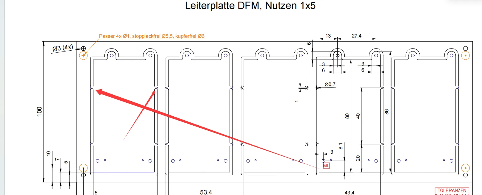
The stamp holes is too small (easy to break). The position of the added stamp perforations is incorrect (there will be a lot of burrs).
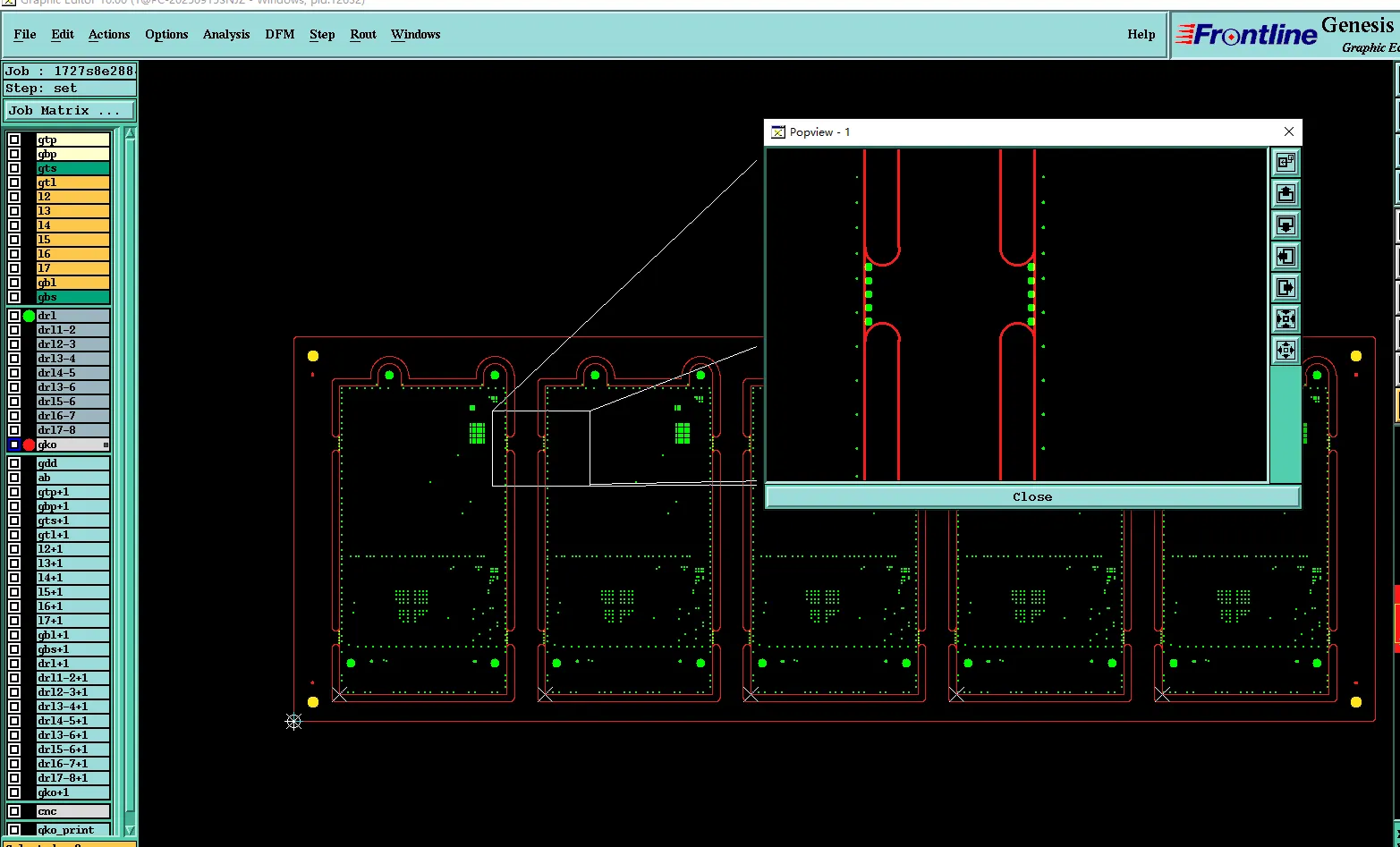
Our company has optimized it as shown in the picture.
The same tab can be wrong on spacing and wrong on position at once. Move the row to clean up the burr and the remaining web often changes with it. The EQ needs both pictures: original hits and proposed hits on the outline and on outer copper, plus a plain statement of what moved — hole count, pitch, inset toward the unit, or location along the edge. If the sketch clips a land, a scored edge, or a connector body that the released files kept clear, that has to be visible before anyone accepts the new positions. Those positions become the production row only after that acceptance.
PCB Stamp Hole Breakage: How CAM Closes Spacing and Position Changes
The three findings close on three decisions. There is no fourth path in which CAM redraws the row to a factory standard pitch.
| EQ wording | What is being decided | Close | What the customer has to confirm |
|---|---|---|---|
| Too small to form a link; factory will delete one stamp hole | Remaining web between adjacent walls on the named tab | Path B — delete one stamp hole | Reduced hole count on that tab; outline unchanged |
| Too small; panel breaks easily / "bridge" position too small | Remaining web and routed tab width versus the handling the package implies | Path A — keep as released, or a named change after the reply | The breakage risk as released, or the requested change to count or tab location |
| Add position wrong; too many burrs; optimized as attached | Hit position on the outline and on outer copper | Path C — accept the factory sketch | The attached positions become the production row |
Path A leaves the released stamp-hole row alone. The customer takes the tight web and the burr condition as they are.
Path B removes one stamp hole on the named tab. Hole count changes; the outline does not. The customer confirms what is left.
Path C accepts the factory sketch. The new positions — and only those positions — become the production row.
On a mixed array one tab can take Path B and another Path C, as long as the EQ names the tabs. Hole diameter, plating, a conversion to V-score, and moving copper to make room are all outside these three paths and stay off the unmarked CAM list.
The updated drill and, for Path C, the accepted sketch go back into the manufacturing package so the next lot does not reopen the same row.
PCB Stamp Hole Design: What to Confirm Before Panel Release
The useful check before release is whether the files agree with each other, not whether the row meets a capability list.
Look at whether the panel drawing and the drill show the same hole count and the same row location on each tab. Look at whether the order note talks about stamp-hole singulation only where the files actually contain the row, or where it clearly asks the factory to add one. Look at whether the outline, the routed channel, and the stamp-hole hits still leave a connecting tab that matches the process the note describes — fabrication only, or through SMT.
The hits should be the stamp-hole tool, not a PTH tool reused on the tab. Copper and silk should sit off the intended break, unless the drawing already accepts a break across that copper. If the factory is going to add or move the row, the package should already be written as if a sketch EQ may come back.
That is the same overlay production CAM will run, applied to the files the customer believes they released.
FAQ
Q1: What is mouse bite in PCB?
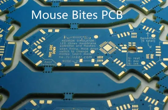
A1: Mouse bites are the same feature this article calls stamp holes: a short row of unplated holes that perforate a breakaway tab so the unit can be snapped out of the panel. The laminate left between those holes is the remaining web, and that web plus the tab width left by routing is what still holds the board to the rail. They are not V-score, not tooling holes on the process edge, and not PTH or component holes that happen to sit on the same outline.
Q2: What are the standard dimensions of PCB mouse bites?
A2: There is no single published dimension set that CAM can apply to every released row. Hole diameter, hole-to-hole spacing, remaining web, and tab width are whatever the panel drawing and the drill actually placed — or whatever a factory sketch later proposes. Review does not replace those files with a standard pitch table. It reads the overlay and then asks the customer to keep the released row, delete one hit, or accept the relocated sketch.
Q3: Is PCB stamp holes spacing the same as tab width or mouse-bite dimensions?
A3: Usually not as one number. Center distance along the row, remaining web between hole walls, and the tab width left by routing are three different lengths. A customer callout for mouse-bite dimensions may be naming any of them. The overlay measures all three and keeps them apart.
Q4: Does an order note that says "stamp holes" or "mouse bites" place the row?
A4: It names the method. Count, tool, and location still need to appear in the drill against the outline, or on a customer panel drawing. If the row exists only on a factory sketch, the EQ should say that.
Q5: If the panel breaks easily, should CAM thicken the connecting tab?
A5: Not on its own. A tab that still exists but looks too weak is a handling question. The customer either accepts the released risk or names a change to hole count, tab location, or singulation method.
Q6: Are stamp holes the same as tooling holes on the process edge?
A6: No. Tooling holes on the rail are for panel handling. Stamp holes perforate the breakaway tab. A PTH or component hole on the same edge is a third tool. Whatever is deleted or moved has to be the stamp-hole tool.