










Engineering Cases
Engineering Cases focuses on real PCB engineering reviews, manufacturing challenges, and production optimization processes from actual fabrication projects. This category highlights how different PCB designs are evaluated and adjusted during engineering review, covering topics such as stack-up analysis, impedance control, drill optimization, copper balancing, solder mask alignment, DFM review, and production risk assessment across various PCB applications. The content in this section is based on practical manufacturing scenarios rather than theoretical introductions. Each engineering case demonstrates how specific PCB issues are identified, analyzed, and resolved during production preparation and fabrication. These records help engineers, purchasers, and hardware teams better understand the relationship between PCB design decisions and manufacturing stability, yield control, and process reliability. Topics may include multilayer PCB engineering review, HDI process optimization, flexible PCB manufacturing considerations, heavy copper processing adjustments, surface finish selection, Gerber data verification, and other real-world PCB production experiences. By organizing engineering challenges and process solutions into structured case content, this category provides valuable insight into practical PCB manufacturing and engineering workflow management.
Featured Blog
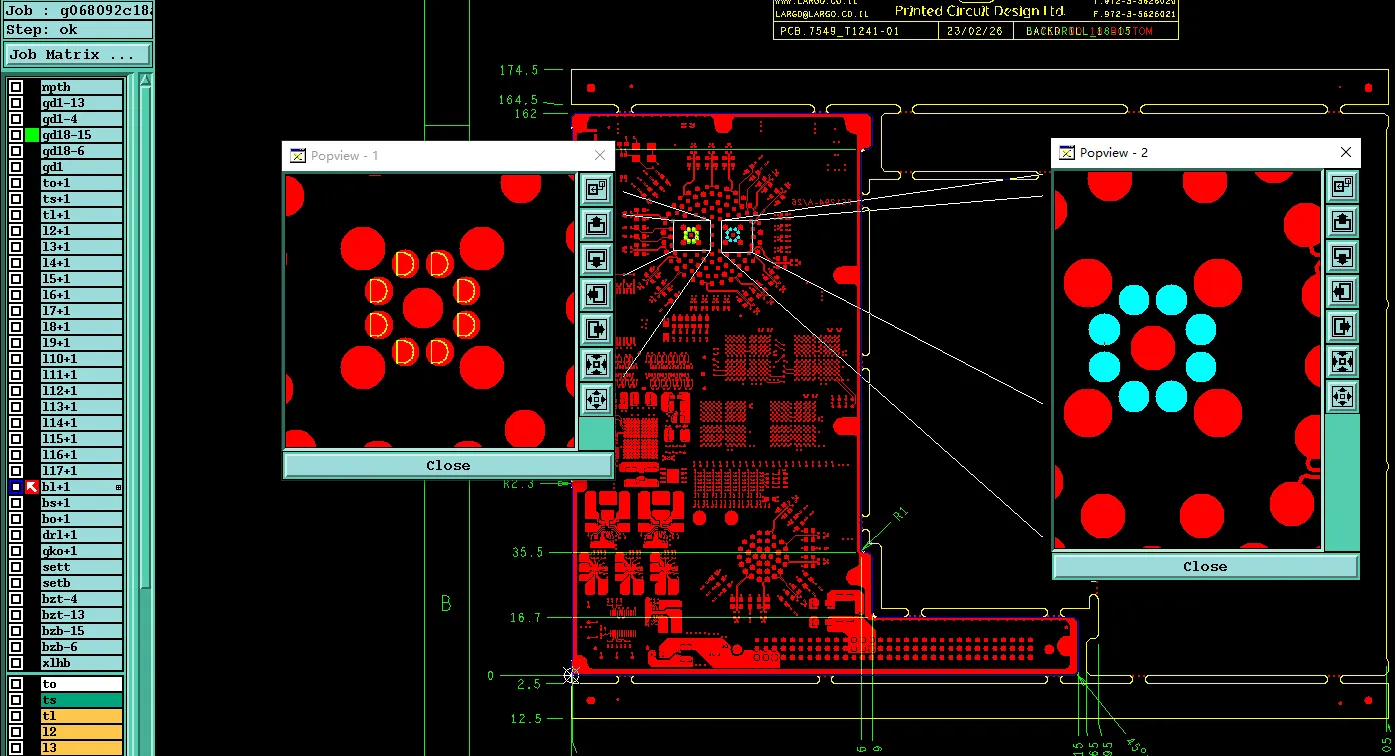
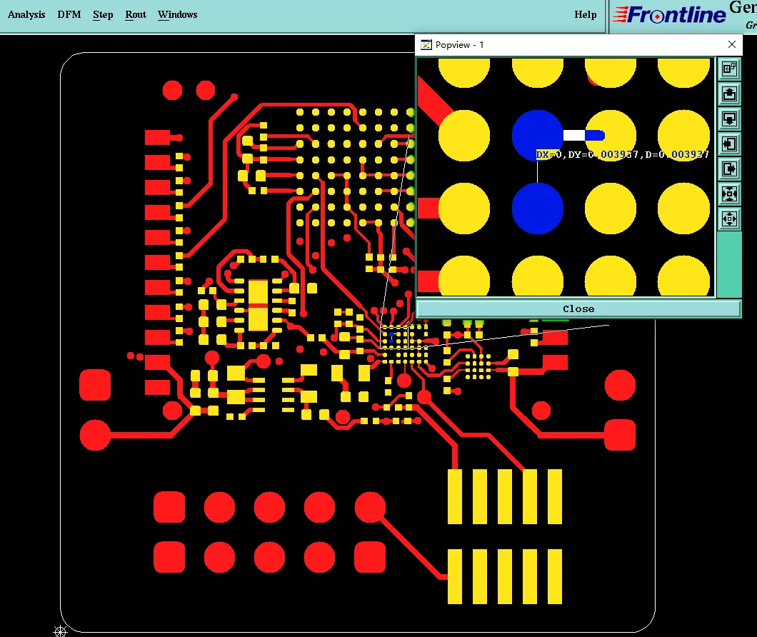
PCB Hole Attributes and Special Drilling: Common CAM Review Conflicts
See how CAM reads PCB hole attributes and special drilling—PTH vs NPTH, back drill, press-fit holes, countersink, and laser vias—and why incomplete data delays fabrication.
Latest Blogs
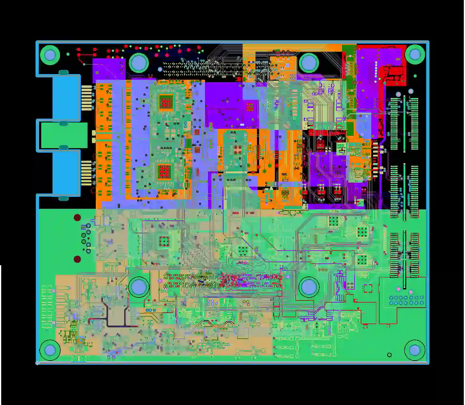
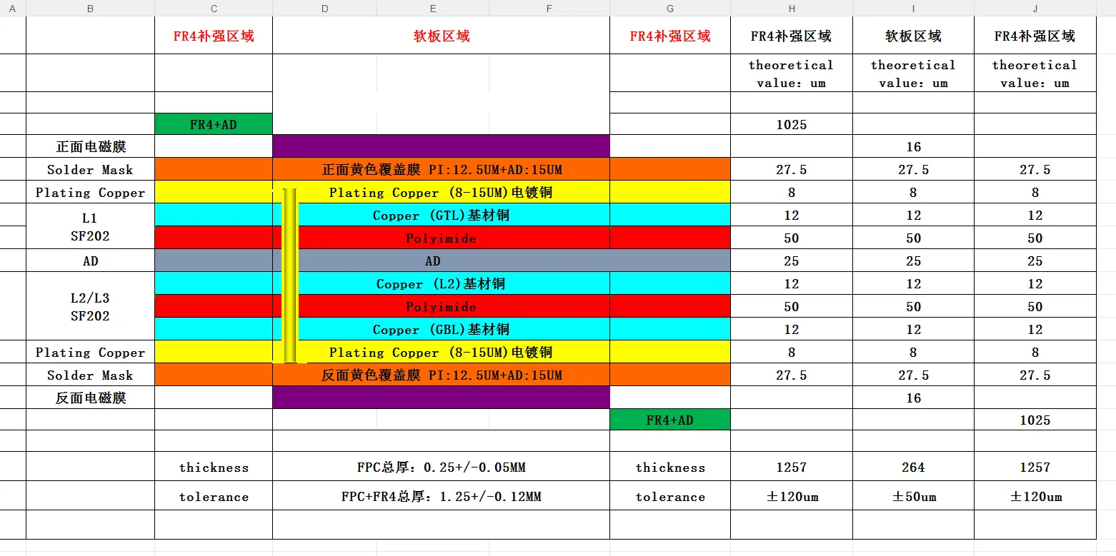
Common PCB CAM Review Engineering Queries in Multilayer HDI PCB Design
Explore common PCB CAM review EQs in Multilayer HDI PCB design, including via spacing, via-in-pad, stack-up, impedance control, and plating issues.
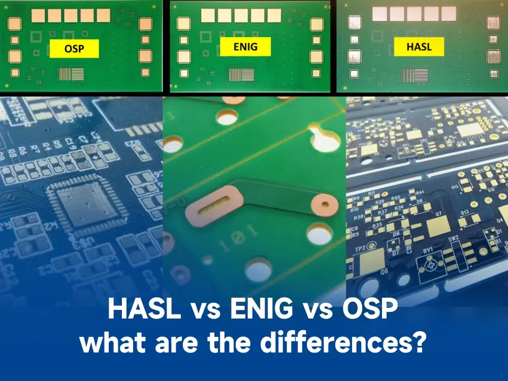
FR4 PCB Surface Finish Guide: ENIG vs HASL vs OSP DFM Issues and Engineering Queries
Explore common engineering queries in ENIG, HASL, and OSP FR4 PCBs. Learn real DFM challenges, surface finish compatibility issues, and practical solutions to reduce manufacturing risks and improve yield.
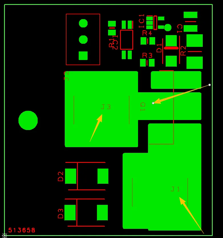
Common Engineering Queries in 2 Layer FR4 PCB Design and Manufacturing
Real Engineering Queries (EQ) and DFM issues for 2 Layer FR4 PCB (double-sided boards) from actual production reviews. Learn how to avoid common problems with via treatment, silkscreen on pads, solder mask openings, hole attributes, board edge clearance, and other frequent design pitfalls.
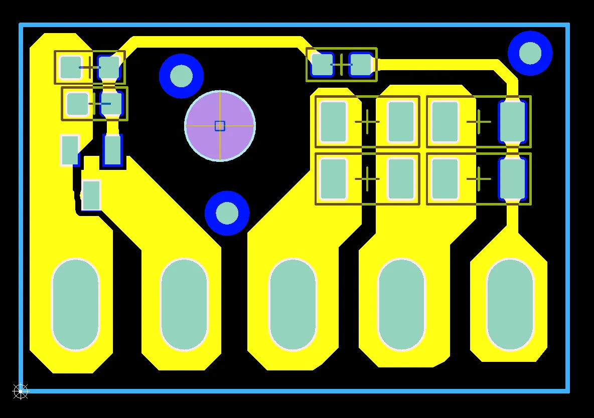
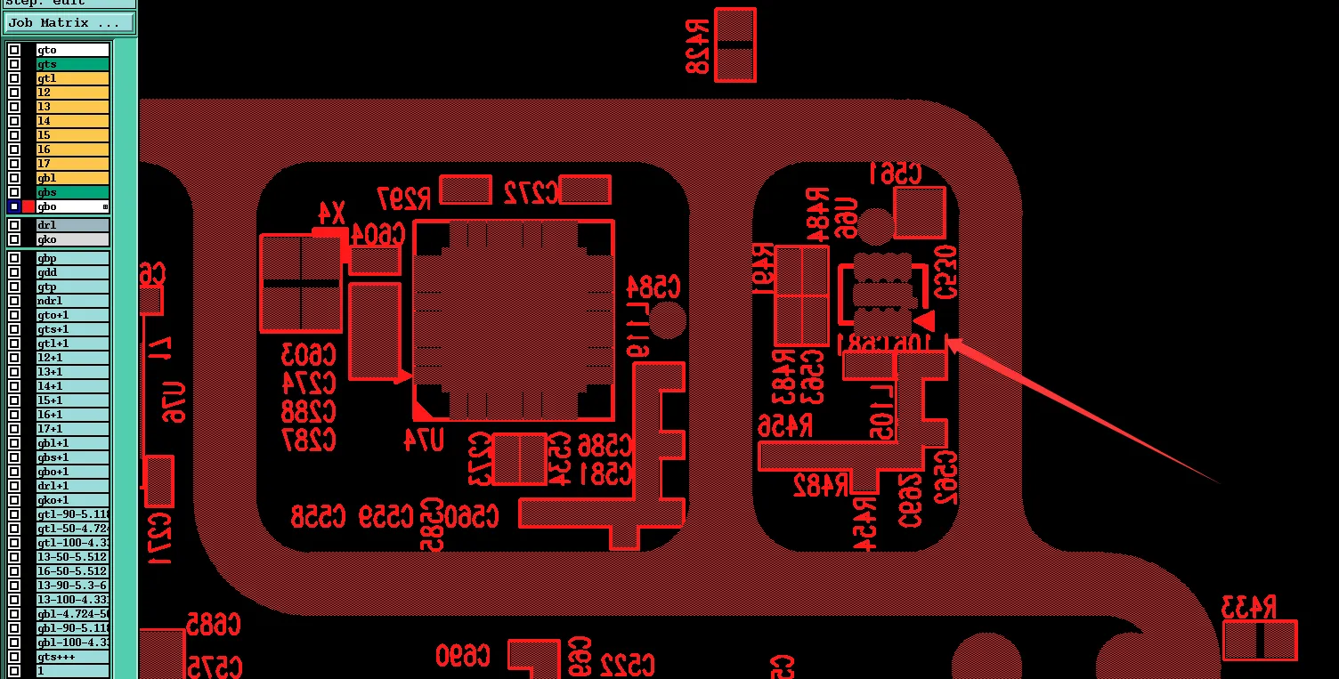
Common 1 Layer FR4 PCB EQ Issues: How Manufacturers Review Gerber Files
Discover the most common engineering queries (EQ) in 1 layer FR4 PCB production, from hole plating confusion to solder mask mismatches. Learn practical file preparation tips to minimize delays and speed up approval.


