


Differential impedance is one of the most important parameters in high-speed PCB design, and it is directly affected by trace spacing, dielectric thickness, and nearby ground structures. In practice, the differential impedance commonly discussed is twice the odd-mode impedance. When the spacing between the two traces of a differential pair increases, the coupling between them gradually weakens, and their ability to suppress common-mode interference is reduced. The magnitude of the impedance change, however, depends strongly on the distance from the signal traces to the reference ground plane. This article examines how differential impedance varies with trace spacing at three dielectric thicknesses, then explains how guard traces placed beside critical signals change the electromagnetic field and lower signal impedance. It also reviews the effect of guard-to-signal spacing and guard trace width, and closes with a twelve-layer board impedance control case that shows why stackup symmetry and impedance continuity matter in real products.
Highlights:
- When the dielectric thickness is small, most of the magnetic field couples to the ground plane, so changing differential trace spacing from 4mil to 26mil may change odd-mode impedance by only about 4 Ω.
- As the signal-to-ground distance increases, coupling between the two traces becomes comparable to or dominant over coupling to ground, so spacing has a much stronger effect on impedance.
- Guard traces provide a low-inductance ground return and reduce crosstalk, but they also lower signal impedance; guard width has a weak and non-monotonic effect, while guard-to-signal spacing and plane spacing determine the strength of the influence.
Differential Impedance Control: Why Trace Spacing Matters
The differential impedance of a pair is twice the odd-mode impedance. To understand how the spacing between the two traces affects differential impedance, it is useful to look at the field distribution. As the distance between the traces increases, the coupling between them gradually weakens, and the pair becomes less effective at suppressing common-mode interference. The amount of impedance change is not the same in every stackup. It depends greatly on the distance between the signal traces and the ground plane, because that distance determines whether the return current and magnetic field are dominated by the ground plane or by the adjacent trace of the pair. These factors should also be considered in EMC design, where differential coupling and common-mode noise behavior influence electromagnetic compatibility.
The following three cases examine the same trend under three dielectric thicknesses: 5mil, 13 mil, and 25 mil. In each case, the differential trace spacing is varied while the rest of the cross-section is held fixed, and the resulting odd-mode impedance is observed.
Differential Impedance Versus Spacing at 5mil Dielectric Thickness
The PCB cross-section of the differential line is shown below.

Figure 6 | PCB structure of differential traces when the dielectric thickness is 5 mil
For a dielectric thickness of 5mil, the effect of differential pair spacing on odd-mode impedance is shown in the following curve.

Figure 7 | Effect of differential line spacing on odd-mode impedance when the dielectric thickness is 5 mil
The curve shows that, over a wide range in which the spacing between the differential traces changes from 4mil to 26mil, the odd-mode impedance decreases by only 4 Ω and finally stabilizes at about 32 Ω. The reason is that when the distance from the signal traces to the ground plane is small, most of the magnetic field lines from the PCB traces couple through the ground plane. The coupling between the two signal traces is therefore relatively weak, and the spacing between them has only a weak effect on odd-mode impedance.
Differential Impedance Versus Spacing at 13 mil Dielectric Thickness
The PCB cross-section of the differential pair is shown below.


Figure 6 | Effect of differential line spacing on odd-mode impedance when the dielectric thickness is 13 mil
The curve shows that when the spacing between the differential traces changes from 4mil to 34mil, the odd-mode impedance increases from 35 Ω to 55 Ω, a change of 20 Ω. Compared with the 5mil dielectric thickness case, the distance from the signal traces to the ground plane is larger. The coupling component between the two signal traces gradually increases and becomes comparable to the coupling to ground. As a result, a change in the spacing between the signal traces has a relatively strong effect on odd-mode impedance.
Differential Impedance Versus Spacing at 25 mil Dielectric Thickness
The PCB cross-section of the differential line is shown below.

Figure 7 | PCB structure of differential traces when the dielectric thickness is 25 mil
For a dielectric thickness of 25 mil, the effect of differential pair spacing on odd-mode impedance is shown in the following curve.
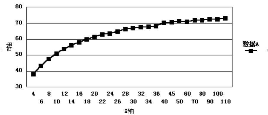
Figure 8 | Effect of differential line spacing on odd-mode impedance when the dielectric thickness is 25 mil
The curve shows that when the distance from the signal traces to the ground plane increases to 25 mil, the coupling between the differential traces plays a decisive role in the overall magnetic field distribution. Although the spacing between the two signal traces is increased to 30mil, which is close to four times the line width, the coupling between the two lines still reduces the impedance by 10 Ω. Therefore, when the distance from the signal to the ground plane is large, the coupling component between differential traces must be taken seriously.
These results also show that when the signal line is far from ground, the differential signal pair has a stronger suppression effect on common-mode interference and reduces the degree of common-mode radiation. For high-speed signal lines, differential signaling should be selected wherever possible, because it can effectively reduce EMI.
Effect of Guard Traces on Impedance
In practical designs, a ground trace, often called a guard line, is frequently added on both sides of a critical signal line. The purpose is to provide a low-inductance ground return path for the critical signal, thereby reducing crosstalk between adjacent lines and reducing conducted and radiated effects. However, adding a guard trace also changes the electromagnetic field distribution around the signal and lowers the impedance of the signal line. The benefit and the penalty therefore need to be evaluated together.
Effect of Guard-to-Signal Spacing on Signal Impedance
To study the effect of guard traces on signals, the following PCB trace structure was set up. The structure is a standard symmetric stripline. Signal+ and Signal- are the positive and negative traces of the differential signal, and guard traces are placed on both sides. The signal trace width is fixed at 8mil, the spacing between the positive and negative signals is 8mil, and the spacing between the two ground planes is 12.50mil or 51.18mil. The PCB structure is shown below.

Figure 9 | PCB structure diagram for studying the effect of ground guarding on signal impedance
When the spacing between the two ground planes is 12.50 mil, the impedance as a function of the guard-to-signal spacing is shown below.
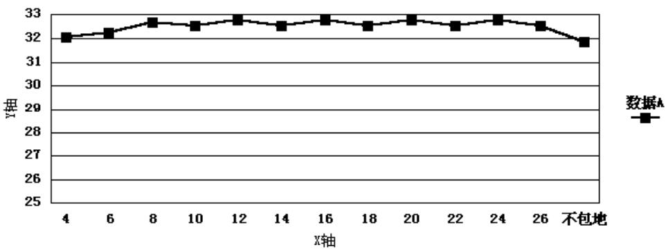
Figure 10 | Effect of ground-to-signal spacing on signal impedance when the spacing between the two ground planes is 12.50 mil
When the spacing between the two ground planes is 27.36 mil, the impedance as a function of the guard-to-signal spacing is shown below.
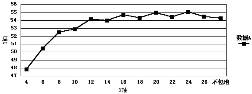
Figure 11 | Effect of ground-to-signal spacing on signal impedance when the spacing between the two ground planes is 27 mil. When the spacing between the two ground planes = 50 mil, the variation of impedance with the spacing between the gr
When the spacing between the two ground planes is 50 mil, the impedance as a function of the guard-to-signal spacing is shown below.
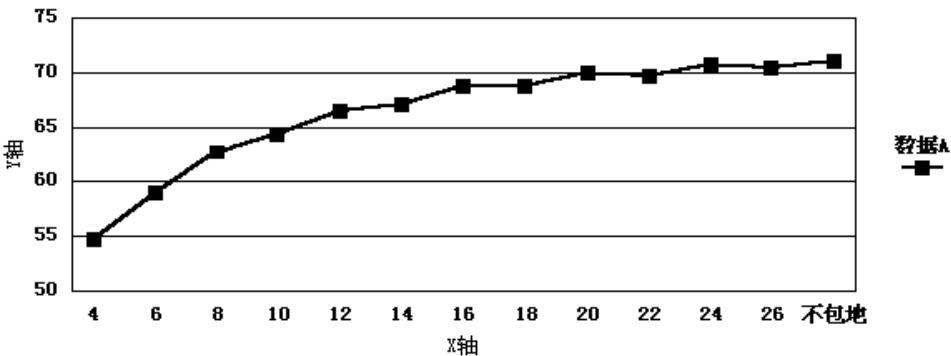
Figure 12 | Effect of ground-to-signal spacing on signal impedance when the spacing between the two ground planes is 50 mil. From the above variation curves, the following can be obtained:
The following conclusions can be drawn from these curves.
- As the distance from the guard trace to the signal trace increases, the effect of the guard trace on signal impedance gradually weakens.
- When the spacing between the two ground planes is 10mil, the signal impedance basically does not change as the guard-to-signal spacing changes from 4mil to 26mil. When the spacing between the two ground planes is 27mil, the signal impedance changes from 48 Ω to 54 Ω as the guard-to-signal spacing changes from 4mil to 26mil. When the spacing between the two ground planes is 50mil, the signal impedance changes from 55 Ω to 70 Ω over the same guard-to-signal spacing range. Therefore, the effect of the guard trace on signal impedance increases as the spacing between the two ground planes increases. This occurs because, as the distance from the signal trace to the ground plane increases, the coupling from the signal trace to the ground plane gradually weakens while the coupling to the guard trace gradually strengthens.
Effect of Guard Trace Width on Impedance
To study the effect of guard trace width on signal trace impedance, the following structure was set up. The signal trace width is fixed at 8mil, the differential signal trace spacing is 8mil, and the spacing between the two ground planes is 27.38mil. The guard-to-signal spacing is 6mil or 12mil.
From the two trends calculated with the XTK simulation software, the following conclusions can be drawn.
A. The effect of guard trace width on signal impedance is not monotonic, and the effect is relatively weak. As the guard trace width changes from 4mil to infinity, the corresponding impedance variation swings within only about 1 Ω. Therefore, in PCB design, a relatively thin ground trace can be used as a shield to save routing space.
B. When the guard-to-signal spacing is 6mil, the single-ended impedance decreases by about 4 Ω and the differential impedance decreases by about 5 Ω. When the distance from the ground trace to the signal is 12mil, the single-ended impedance decreases by about 1 Ω and the differential impedance also decreases by about 1 Ω.
For critical signal lines and interface signals, guard traces can be considered for shielding. The guard structure should be evaluated with the actual stackup, because its effect depends on the distance to the reference planes and on the spacing between the guard and the signal.
Impedance Control Case Study: A Twelve-Layer Board
The following case shows impedance control on a product board. The board structure is shown below.

The board is a twelve-layer board with six routing layers. The ground layers are GND1, GND2, and GND3. The power layers are VCC1, VCC2, and VCC3. VCC1 is a +5 V power layer, VCC2 is a +3.3 V power layer, and VCC3 is a 1.5V power layer. The figure shows that the inner-layer transmission line impedance is 35 Ω and the top-layer impedance is 49 Ω. The inner and outer layer impedances are therefore discontinuous. Under this layer structure, the data lines from SD535 to the B port of GTL16923 are difficult to match, causing step and overshoot. This phenomenon cannot be eliminated by matching. Such impedance discontinuities and signal integrity issues should be carefully considered in RF PCB Routing, particularly when signals transition between layers with different characteristic impedances.
After the board change, the board structure is as follows.
| Layer | Material | Thickness (mm) | Thickness (mil) | Impedance |
|---|---|---|---|---|
| Top | 2*1080 | 0.14 mm | 5.52 mil | 53 Ω |
| GND1 VCC1 | 0.1 mm | |||
| Art04 | 2*2116 | 0.22 mm | 8.66 mil | 50 Ω |
| Art05 | 0.2 mm | 50 Ω | ||
| 2*2116 | ||||
| GND2 | 0.1 mm | |||
| VCC2 Art08 | 2*2116 | 50 Ω | ||
| Art09 | 0.2 mm | 50 Ω | ||
| VCC3 | 2*2116 | |||
| GND3 | 0.1 mm | |||
| Bottom | 2*1080 | 53 Ω |
The original structure, in which two planes sandwiched one signal layer, was changed to a structure in which two planes sandwich two signal layers. This makes the inner and outer layer impedances basically consistent and eliminates the step and overshoot on the data lines between SD535 and GTL1655. The disadvantage of this structure is that crosstalk exists between adjacent signal layers. Crosstalk between adjacent signal layers can be reduced by routing adjacent layers orthogonally and by limiting the length of parallel routing.
The PCB thickness is 2.2mm ±10%. On the PCB, the line width is basically 8mil, the clock line width is 10mil, and the line spacing is 7mil.
The impedance control for the transmission lines on each layer is as follows.
Top and bottom layer impedance: 50 Ω ±10% at 8mil line width, and 45 Ω ±10% at 10mil line width.
Inner-layer impedance: 49 Ω ±10% at 7mil line width, 46 Ω ±10% at 8mil line width, and 41 Ω ±10% at 10mil line width.
Related Reading:
- Capacitor Selection and Placement for PCB EMC Design
- Transmission Line Models: Microstrip, Stripline, and Reflections
- Surface Microstrip vs. Inner-Layer Stripline Routing
- Impedance Control Basics: Characteristic Impedance Explained
- Special Signal Handling and Via Effects in PCB Design
- Backplane Slot Layout and Board Position Structure for EMC Design
- Backplane Connector, Impedance, and Power/Ground Design for EMC
- PCB EMC Design: Module Partitioning and Special Component Layout



