 00:53
EMI Reduction
Electromagnetic interference (EMI) poses a significant challenge in modern electronics design, where unwanted signals can disrupt circuit performance, lead to compliance failures, or cause system malfunctions. The EMI Reduction tag on this blog aggregates expert insights and practical strategies to help engineers and hobbyists effectively minimize these issues in printed circuit boards (PCBs) and electronic assemblies. By focusing on proven methods, this collection addresses the core needs of professionals seeking to enhance signal integrity, meet regulatory standards like FCC or CE, and optimize device reliability in noisy environments. Key topics under EMI Reduction include essential techniques such as proper PCB layout optimization, where trace routing and component placement play critical roles in reducing crosstalk and radiated emissions. Grounding practices, for instance, involve creating low-impedance paths to shunt noise away from sensitive areas, while shielding enclosures and ferrite beads offer straightforward ways to suppress high-frequency interference. Readers will find discussions on filtering solutions, like using capacitors and inductors to attenuate unwanted frequencies, alongside real-world case studies that demonstrate how these approaches resolve common problems in consumer electronics, automotive systems, and industrial controls. For those troubleshooting persistent EMI issues or designing new prototypes, the articles here provide actionable steps, from selecting appropriate materials to simulating designs with tools like SPICE or electromagnetic field solvers. Implementing these best practices not only prevents costly redesigns but also ensures robust performance in electromagnetic compatibility (EMC) testing. As you delve into the posts linked below, you'll gain the knowledge to apply these concepts directly to your projects, fostering innovation in interference-free electronics.
Video Guide

Technical Articles
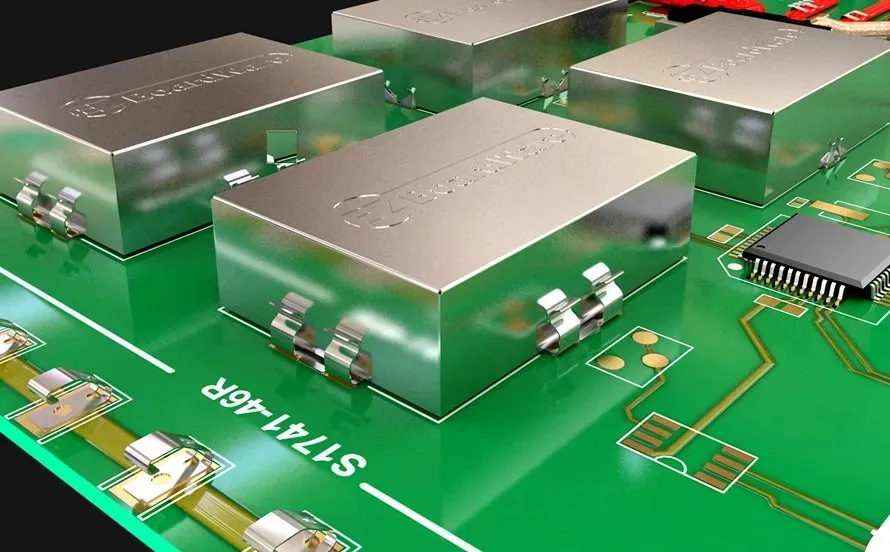
PCB Component Placement for EMC Compliance: Reducing Interference
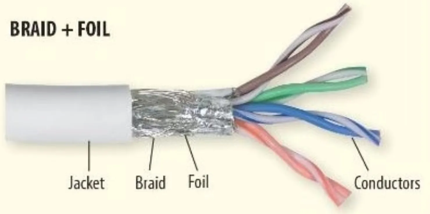
Mastering Cable Shielding: Types, Techniques, and Best Practices
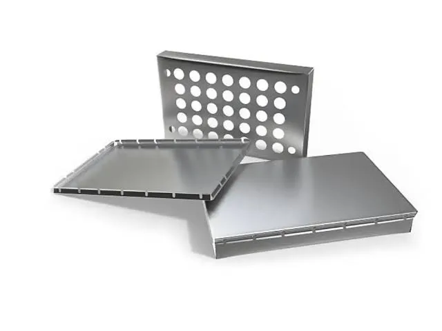
EMI Shielding Design Guide for Sheet Metal Enclosures
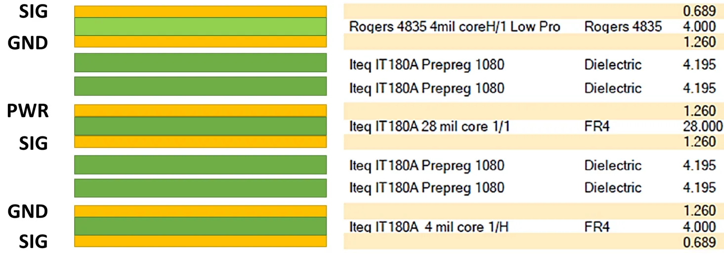
PCB Stackup for EMC: Best Practices for Reducing Electromagnetic Interference
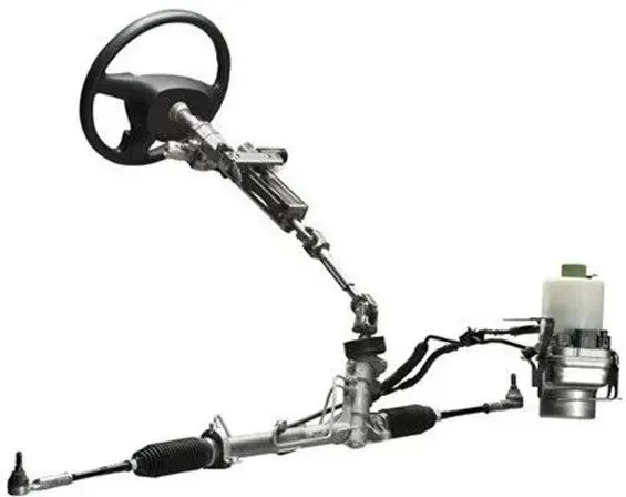
Steer-by-Wire and Intelligent Chassis Systems: PCB Design, Redundancy, and High-Reliability Challenges for Next-Generation Vehicles
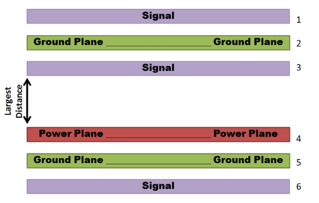
The Art of Layering: Signal Layer Strategies for PCB Success

DIY Home Medical Kit: Front-end Amplifier and EMI
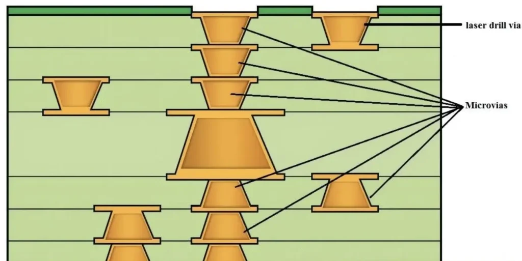
Microvia Design for EMI Reduction
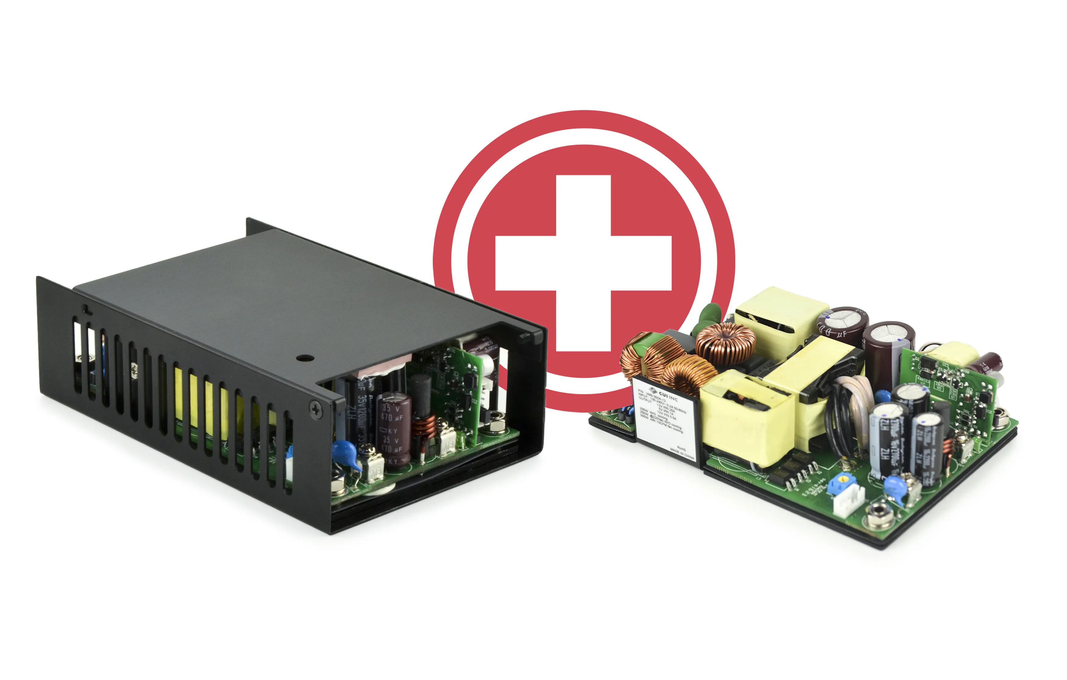
Medical power supplies with secondary DC/DC isolation
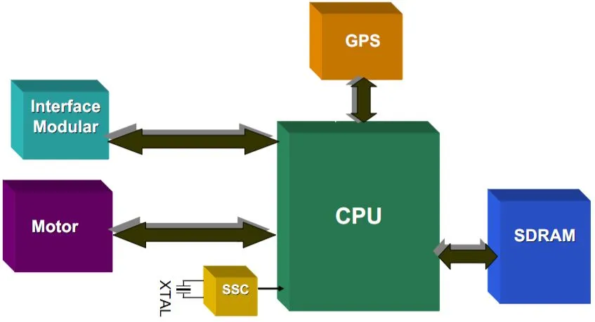
Near-Field EMI Testing for Drone Platforms: EMC Strategies and PCB Design Insights

Core Concepts and Methods of Counter-UAS Technology
High-Voltage Wiring Design for New-Energy Vehicles
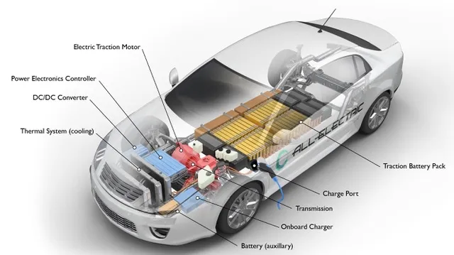
High-Voltage PCB Design for Electric Vehicles: 800V Platforms, Battery Management, and Power Distribution Systems
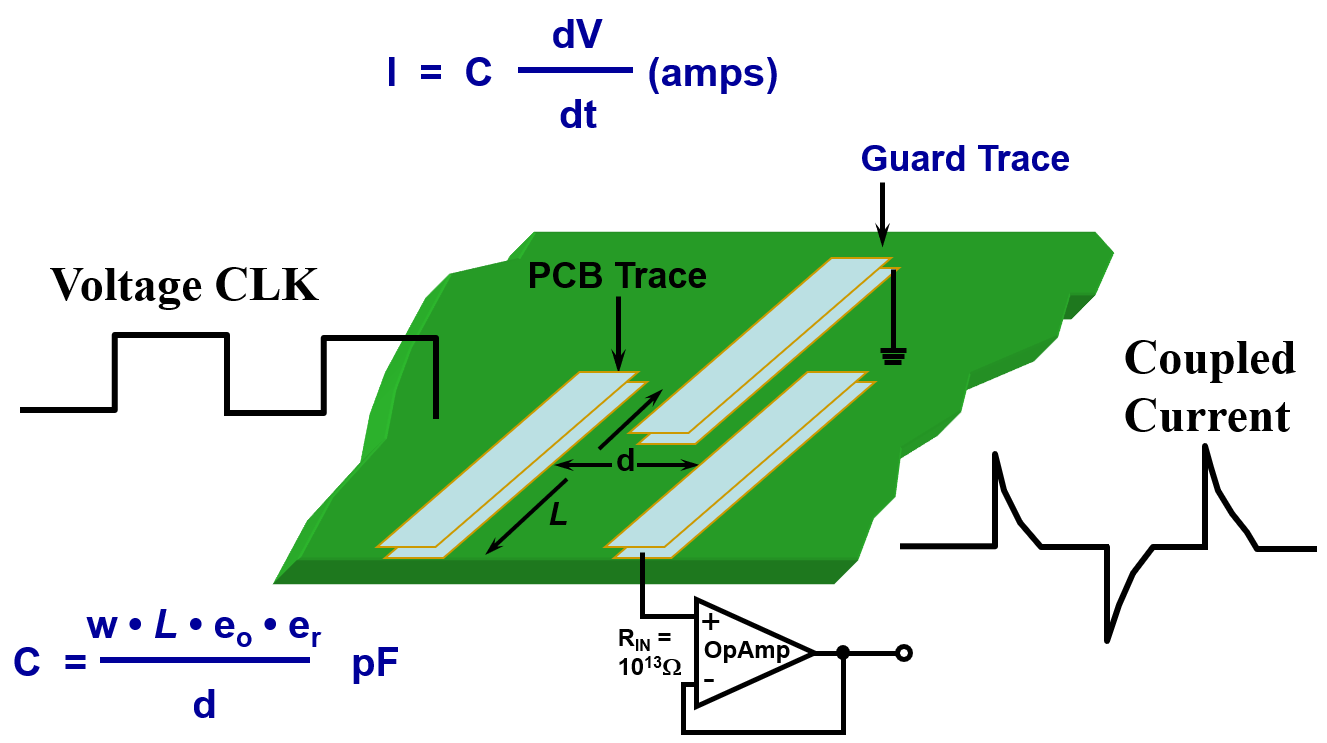
Reducing EMI in PCB Prototyping: Shielding Techniques and Grounding Strategies
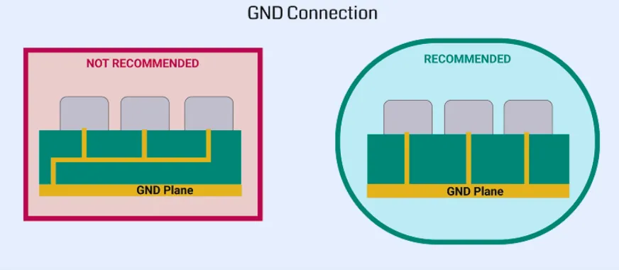
PCB Grounding Techniques: A Guide to Minimizing Noise and Ensuring Reliable Connections
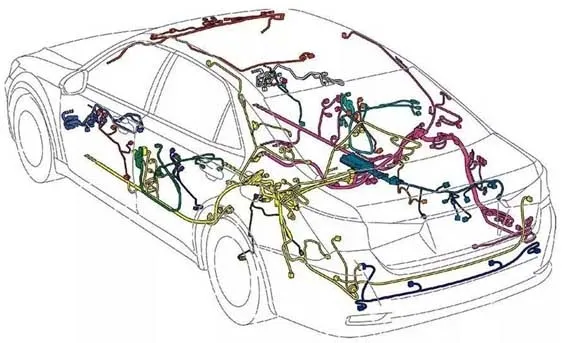
Grounding Design for Automotive Wiring Harnesses
CentOS 7 Firewall: firewalld and iptables Examples
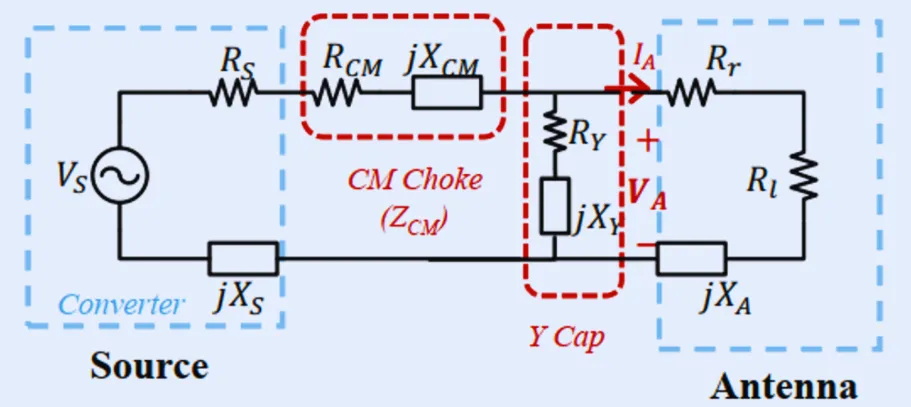
Capacitors in EMC Design: A Deep Dive into Filtering and Noise Suppression

Essential MOSFET Gate Driver Designs for Reliable Power Systems