Impedance Control
Impedance control is a critical aspect of printed circuit board (PCB) design, ensuring that signal traces maintain consistent electrical characteristics to prevent distortions, reflections, and data loss in high-speed applications. This tag encompasses a range of topics related to managing characteristic impedance in PCBs, from fundamental concepts to advanced implementation strategies. For engineers and designers searching for impedance control solutions, understanding this principle is essential for optimizing performance in systems like telecommunications, computing, and automotive electronics, where signal integrity directly impacts reliability and efficiency. At its core, impedance control involves precise calculation and control of trace geometry, dielectric materials, and layer stackups to match the required impedance values, typically 50 ohms for RF signals or 100 ohms for differential pairs. Practical applications include high-speed interfaces such as USB, PCIe, and Ethernet, where mismatches can lead to electromagnetic interference or signal degradation. Best practices start with accurate simulations using tools like field solvers to predict impedance, followed by selecting appropriate trace widths, spacing, and via configurations. For instance, maintaining uniform trace routing and incorporating ground planes can minimize variations, while regular testing with time-domain reflectometry ensures compliance during prototyping. Professionals often encounter challenges like manufacturing tolerances or environmental factors affecting impedance, which this tag addresses through case studies and troubleshooting guides. By delving into these resources, you can gain actionable insights to refine your designs, such as integrating controlled impedance into multilayer boards or adapting to flexible PCBs. Exploring the articles under this tag provides in-depth discussions on these techniques, helping you apply proven methods to your projects and achieve robust, high-performance electronics.
Technical Articles

Five Key Points for 5G Testing
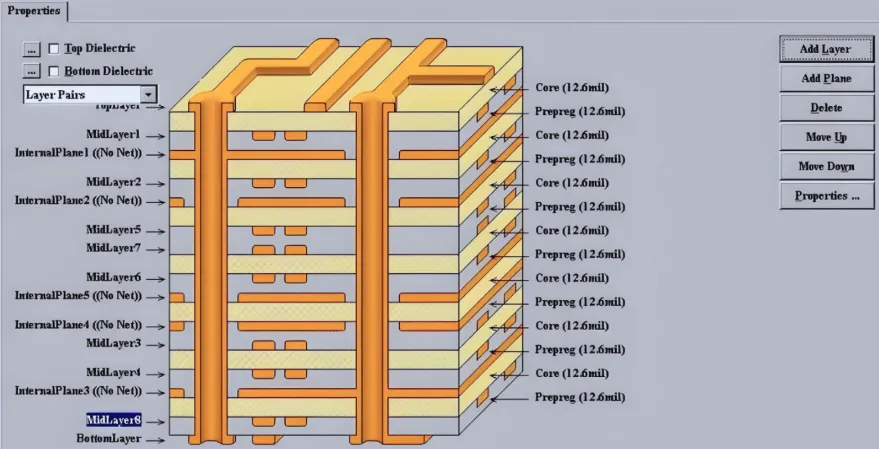
Optimizing PCB Performance: The Impact of Prepreg Thickness and Dielectric Constant
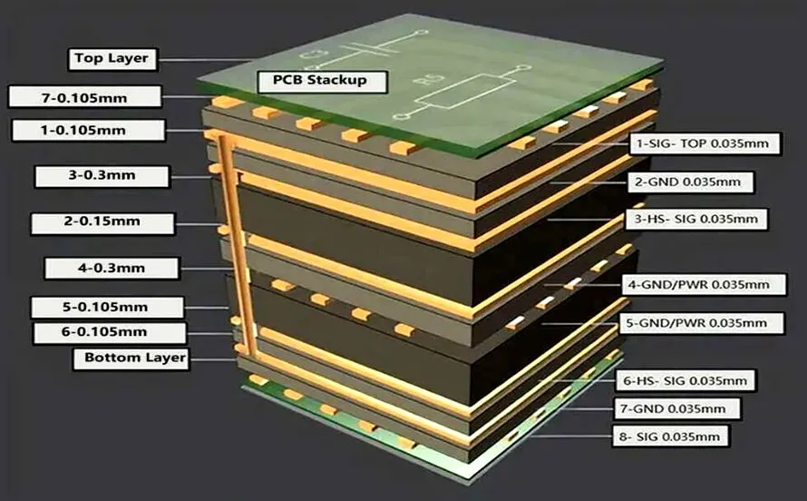
Unleashing PCB Performance: A Guide to Asymmetrical Stackup Design
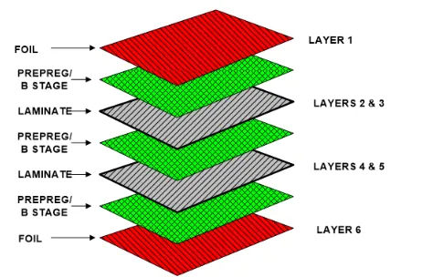
Optimizing ECU PCB Performance: A Guide to Layer Stackup Design
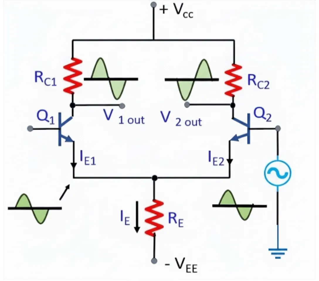
Differential Amplifier Basics: Principles, Formulas, Circuits, and PCB Design Insights
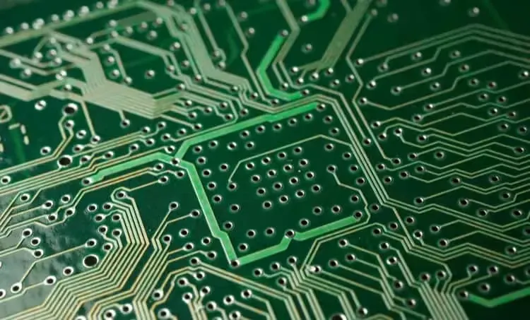
Mastering PCB Impedance Simulation for High-Speed Designs
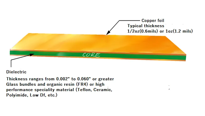
Dielectric Thickness and Impedance: A PCB Design Essential
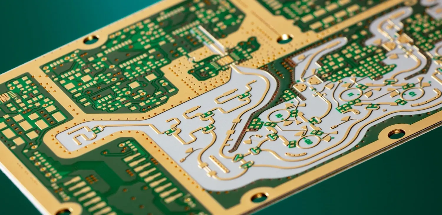
Rogers PCB for High Frequency Amplifiers: Design Considerations
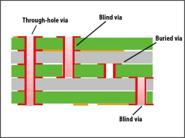
Blind Vias in PCB Design: Optimizing High-Density Boards
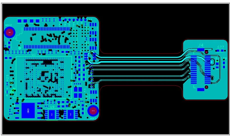
Video Processing PCB Design: A Comprehensive Guide for Beginners
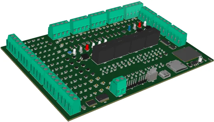
Unlock Signal Integrity: The Ultimate Guide to 8-Layer PCB Stackup Design
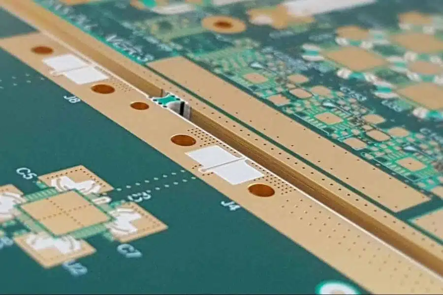
Mastering 12-Layer PCB Stackups for High-Performance High-Speed Designs
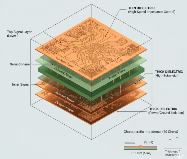
Optimizing Dielectric Thickness in Multilayer PCBs for Enhanced Performance

5G and PCB Mass Production: Designing for High-Speed Connectivity
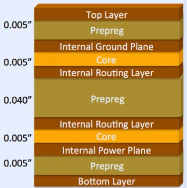
Choosing the Right PCB Layer Thickness: A Comprehensive Guide
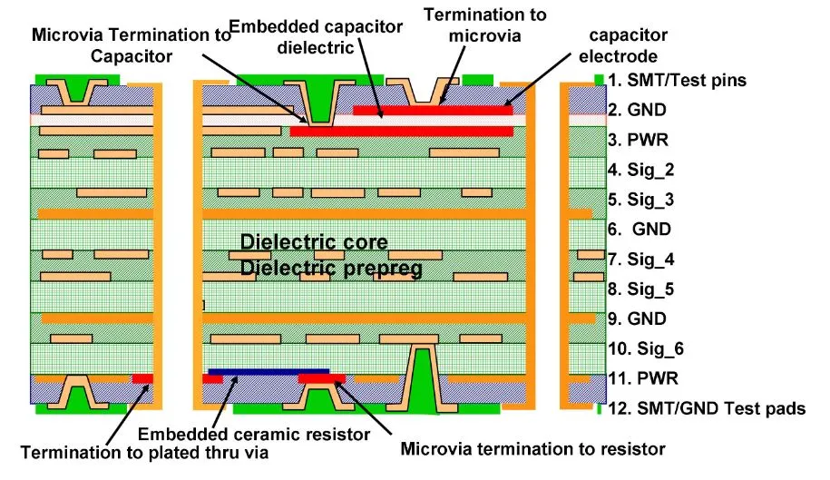
Advanced HDI PCB Stackup Materials for Improved Signal Performance
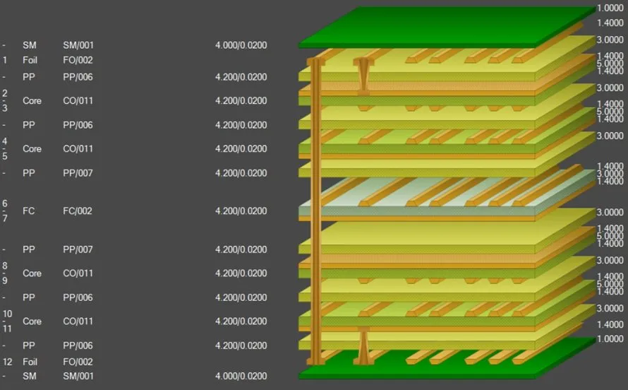
Understanding The PCB Stackup
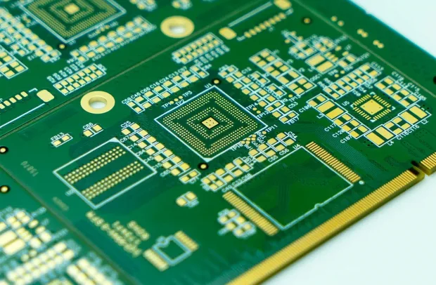
Mastering 4-Layer PCB Design: A Comprehensive Guide to Layout & Stackup