 00:54
Multilayer PCB Design
Multilayer PCB design represents a critical advancement in printed circuit board technology, enabling engineers and designers to create compact, high-performance electronic systems. Unlike single or double-layer boards, multilayer PCBs incorporate multiple layers of conductive traces separated by insulating materials, allowing for intricate routing, reduced electromagnetic interference, and improved signal integrity. This approach is essential for modern applications where space constraints and functionality demands are high, such as in smartphones, medical devices, automotive electronics, and aerospace systems. For professionals and hobbyists searching for multilayer PCB design resources, this tag serves as a comprehensive hub, offering insights into optimizing layer counts, managing thermal dissipation, and ensuring manufacturability. Key best practices highlighted in our articles include strategic layer stacking to minimize crosstalk, selecting appropriate via types like blind or buried vias for efficient interconnections, and implementing controlled impedance for high-speed signals. Readers can find practical guidance on using design software tools like Altium or KiCad to simulate and validate multilayer layouts, along with tips for cost-effective prototyping and compliance with industry standards such as IPC-2221. By addressing common challenges like signal routing density and power distribution, these resources empower users to tackle real-world projects with confidence. Whether you are refining a prototype or scaling production, the content under this tag provides actionable strategies to enhance reliability and performance. Delve into specific case studies and tutorials to apply these concepts directly to your work, fostering innovation in your PCB endeavors.
Video Guide
Technical Articles
Industrial Instrumentation Guide and Selection
High Tg PCB Manufacturing: Design Tips for Optimal Performance

NB-IoT PCB Design and Manufacturing for IoT and Smart Home Devices

High-Security Cryptographic Module Design Architecture
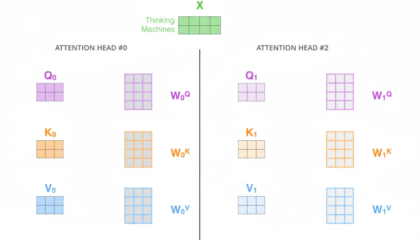
Transformer Model Implementation Details
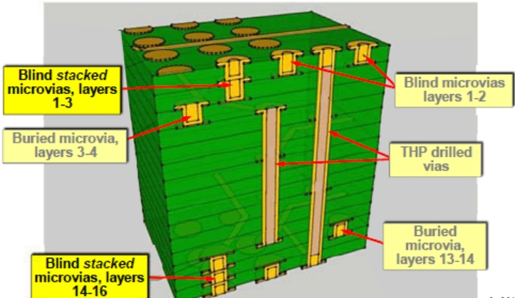
Reducing EMI in High Layer Count PCBs: Shielding and Grounding Techniques
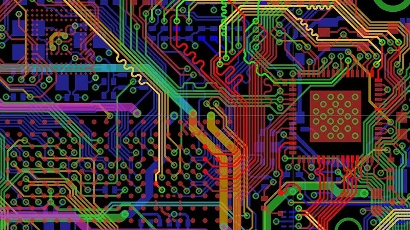
8 Layer PCB Stackup: Structure, Examples, and Design Considerations

Development of Embodied-Intelligence Mobile Manipulators
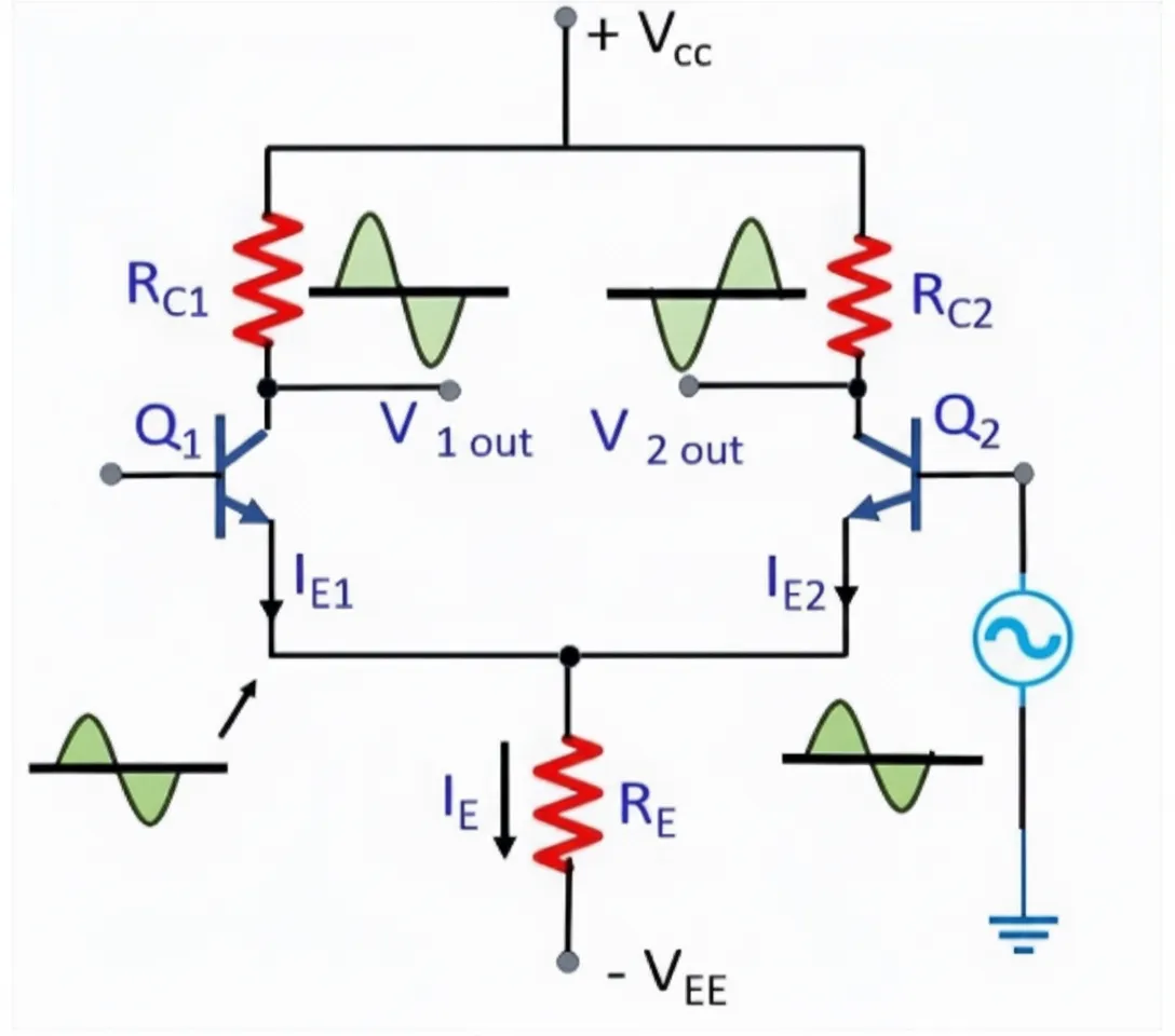
Differential Amplifier Basics: Principles, Formulas, Circuits, and PCB Design Insights
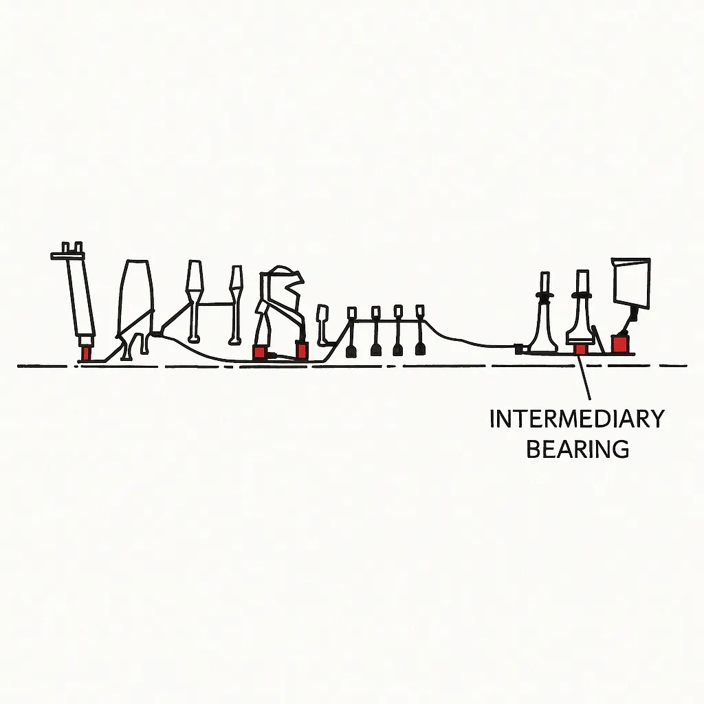
Evolution of High-Speed Rotors in Aircraft Engines
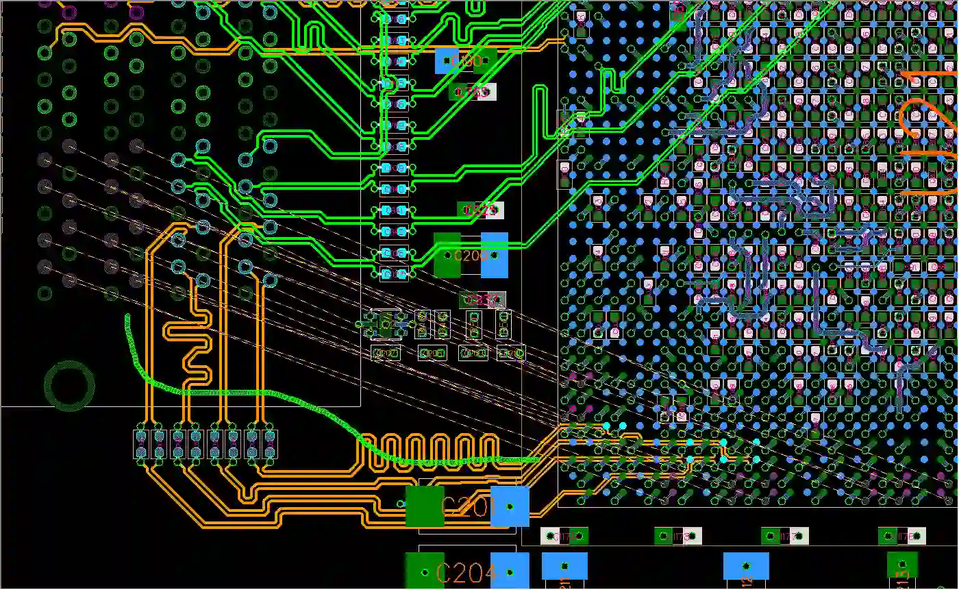
Designing Your First Router PCB: A Beginner's Comprehensive Guide
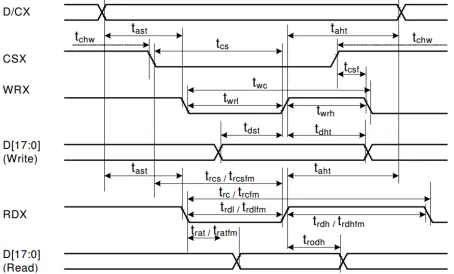
STM32 FSMC LCD Interface and Timing
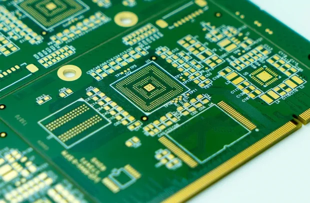
Mastering 4-Layer PCB Design: A Comprehensive Guide to Layout & Stackup
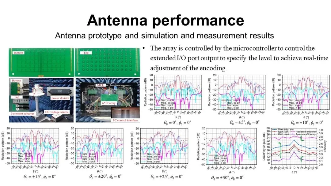
Low-Profile Dual-Polarized Dual-Beam Scanning Antenna Array
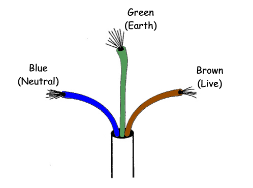
Why the Neutral Wire Can't Be Replaced by Earth
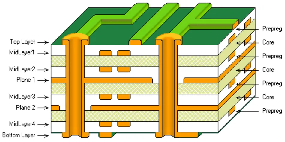
Multi-Layer PCBs: A Beginner's Guide to Design and Fabrication
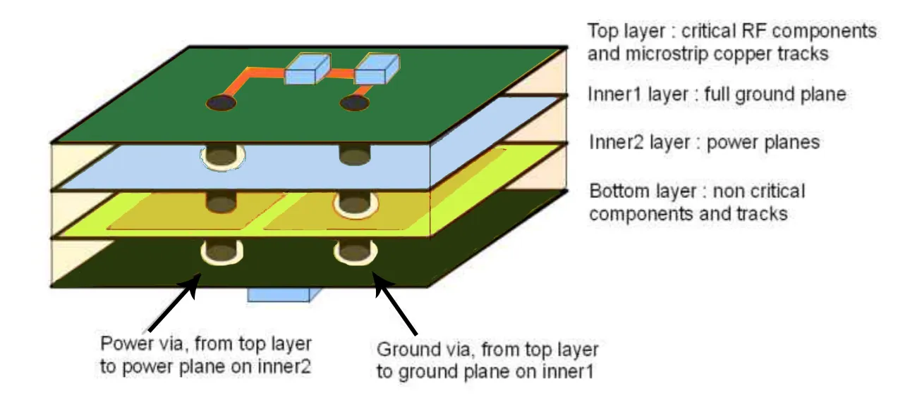
Routing Challenges and Solutions on 4-Layer PCBs
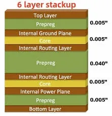
6 Layer PCB Design Guidelines for EMI/EMC Compliance
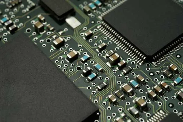
The Future of 6-Layer PCBs: Trends and Innovations in PCB Technology