


PCB Design
Printed Circuit Board (PCB) design forms the backbone of modern electronics, enabling the creation of compact, efficient, and reliable devices that power everything from smartphones to industrial machinery. In this category, readers gain access to a comprehensive collection of resources dedicated to mastering PCB design principles and techniques. Whether you are a seasoned engineer refining complex layouts or a newcomer learning the fundamentals, these articles provide the knowledge needed to tackle real-world challenges in electronics development. The scope of PCB design covered here extends from initial schematic capture to final board fabrication and testing. Articles delve into essential topics such as layer stacking, signal integrity, thermal management, and component placement strategies. Guides and tutorials offer step-by-step instructions for using popular software tools like Altium Designer and KiCad, while insights explore emerging trends like flexible PCBs and high-speed designs. Best practices emphasize error reduction, cost optimization, and compliance with industry standards, ensuring designs are not only functional but also manufacturable at scale. Real-world applications highlight the category's practical value, demonstrating how effective PCB design contributes to innovations in automotive systems, medical equipment, renewable energy solutions, and consumer gadgets. By addressing common pitfalls and sharing expert tips, these pieces equip professionals to enhance product performance and reliability. Readers benefit from building a deeper understanding through interconnected articles that cover foundational concepts alongside advanced methodologies, fostering continuous improvement in electronics projects. For those involved in prototyping or production, the technical relevance of this content lies in its focus on efficiency and innovation. Detailed discussions on impedance control, EMI shielding, and design for manufacturability prepare you to meet the demands of today's fast-paced tech landscape. Engaging with multiple articles in this category allows for a progressive learning path, where foundational knowledge supports exploration of specialized topics, ultimately leading to more robust and innovative PCB designs.
Featured Blog
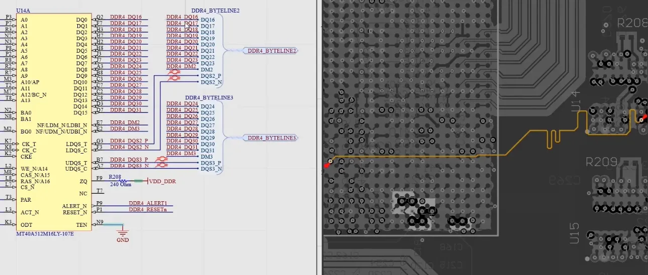
PCB Design Review for Beginners: A Step by Step Guide
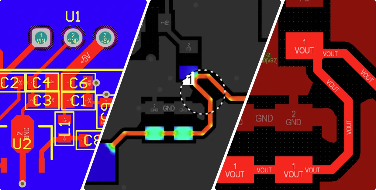
Learn how to perform a PCB design review with a practical checklist covering schematics, layout, DRC, manufacturability, and pre-production checks.
Latest Blogs
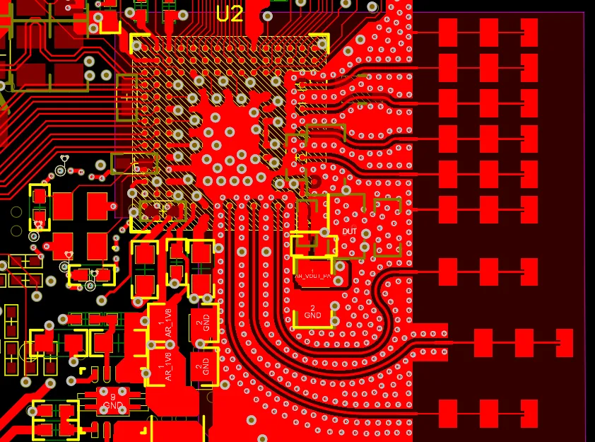
Optimizing PCB Stack Up for RF Applications: A Practical Guide
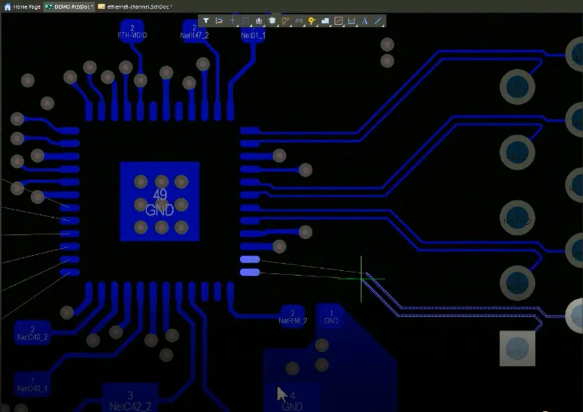
Master RF PCB stack-up optimization with this practical guide. Learn impedance control, low-loss material selection, symmetrical layering, and antenna integration strategies to reduce signal loss and achieve first-pass success in 5G, radar, and mmWave designs per IPC-2228 standards.
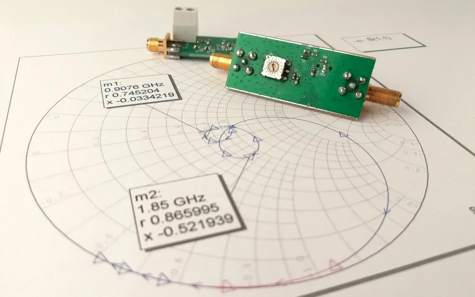
Silkscreen Design Mistakes to Avoid: Ensuring Error Free PCB Assembly
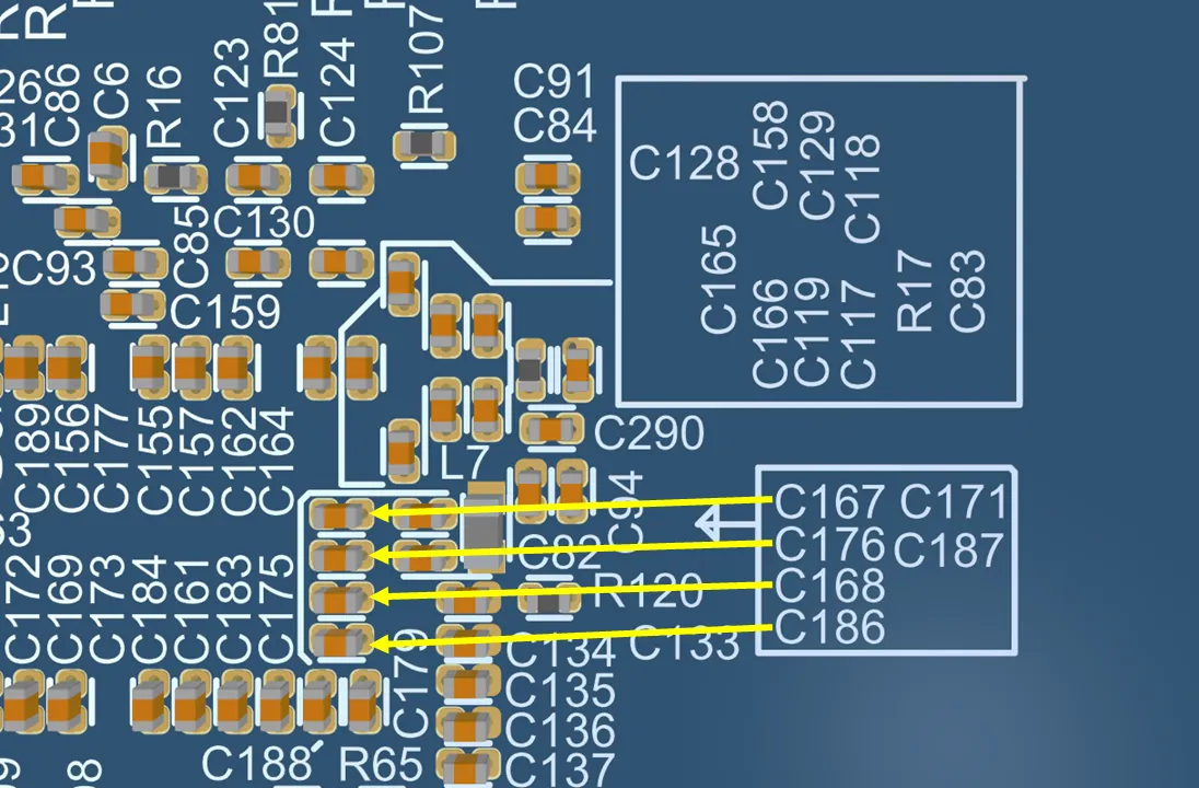
Fix PCB silkscreen errors like over pads, over vias, misplacement, and readability issues to ensure error-free assembly. Practical tips for electrical engineers on silkscreen design flaws, clearances, and best practices for reliable PCB production and fewer defects.
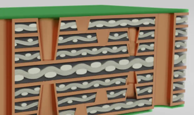
The Ultimate Guide to Silkscreen Fonts: Choosing the Right Typeface for PCB Manufacturing
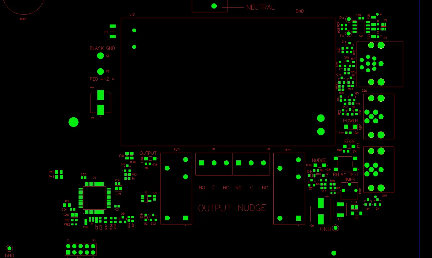
Choosing the best PCB silkscreen fonts improves PCB readability and manufacturing efficiency. This guide covers readable PCB fonts, font size guidelines, silkscreen standards, placement best practices, and troubleshooting for clear markings that last through assembly and testing.
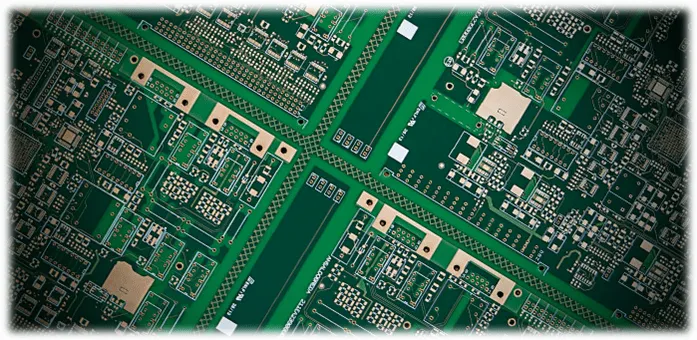
Silkscreen Design for High Density PCBs: Achieving Clarity in Compact Spaces
Master silkscreen design for high-density PCBs with practical guidelines on clearances, font sizes, layout strategies, and alternatives like laser marking. Achieve clear component identification in tight spaces while improving assembly accuracy and manufacturability.
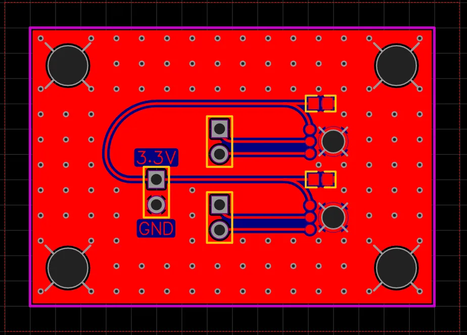
Mastering PCB Copper Pour: Techniques for Effective Grounding and Noise Reduction
Achieve better signal integrity with PCB copper pour grounding techniques that cut noise and strengthen ground planes. Learn practical steps for copper pour noise reduction, ground plane copper pour implementation, and minimizing ground loops copper pour in high-speed PCB designs for electric engineers.
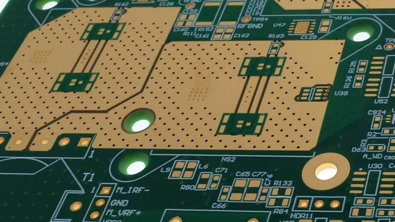
Thermal Management in PCBs: How Copper Pour Layout Enhances Heat Dissipation
Discover how copper pour layout enhances heat dissipation in PCB thermal management. Learn technical principles, best practices, and troubleshooting for high-power designs — reduce hotspots and improve reliability with proven copper pour strategies.
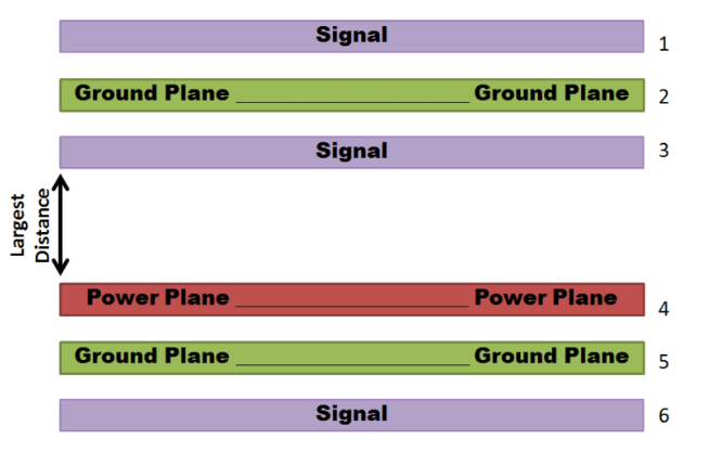
Mastering PCB Ground Plane Design for High-Speed Signal Integrity
Master PCB ground plane design for high-speed circuits. Learn why proper ground planes are critical for signal integrity, EMI reduction, and reliable return paths. Discover proven strategies used by professional PCB designers.
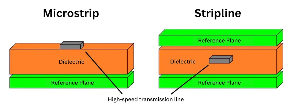
Advanced PCB Impedance Control: Techniques for Minimizing Signal Loss
Master advanced PCB impedance control techniques to minimize signal loss in high-speed designs. Learn stackup optimization, material selection, routing strategies, via innovations, and verification methods for superior signal integrity and reduced reflections.
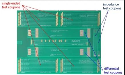
PCB Impedance Control Testing: Ensuring Compliance with Design Specifications
PCB impedance control testing verifies trace performance against design specs using TDR and VNA methods. Review equipment, PCB testing standards like IPC, best practices, troubleshooting, and verification steps for signal integrity and manufacturing compliance in high-speed electronics. Ideal for electrical engineers.
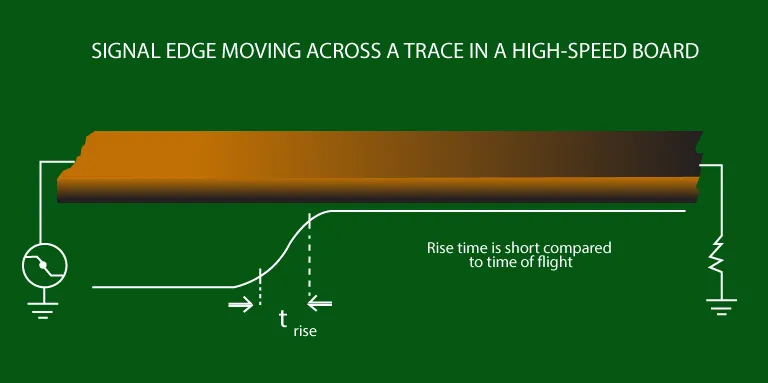
Demystifying PCB Impedance: A Beginner's Guide to Controlled Impedance Design
Demystify PCB impedance with this beginner-friendly guide to controlled impedance design. Learn microstrip vs stripline, stackup basics, simple calculations, free tools, common mistakes, and how to specify impedance for reliable high-speed PCB manufacturing.
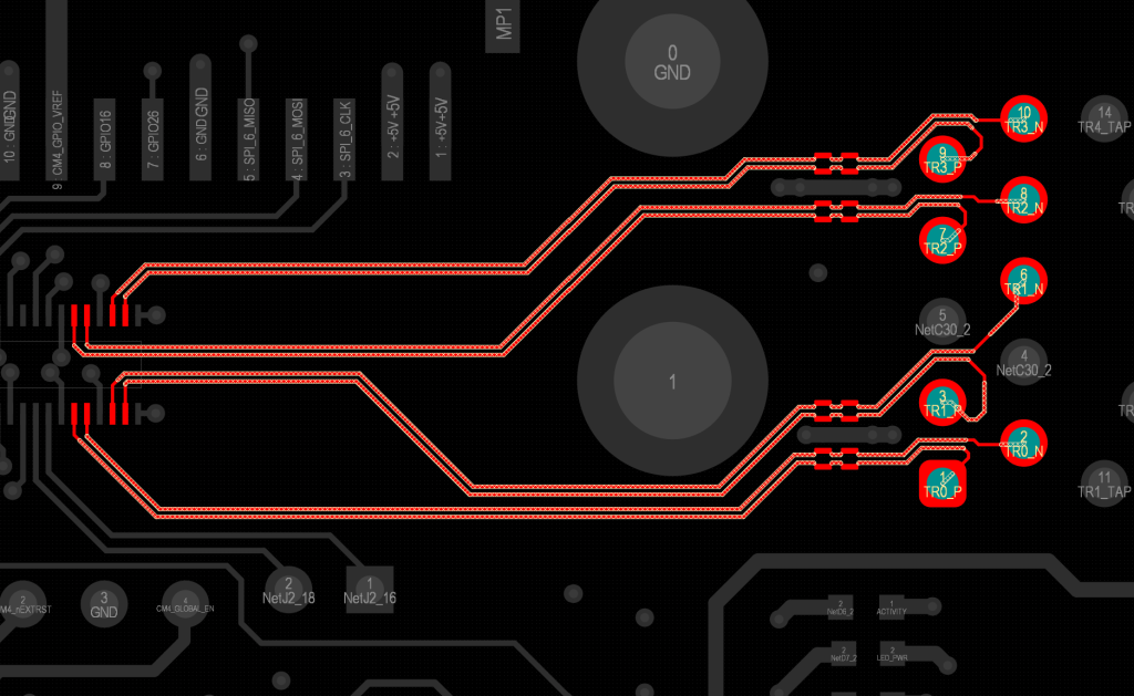
Via Placement for Differential Pairs: Maintaining Impedance and Signal Integrity
Learn proven via placement strategies for differential pairs to maintain controlled impedance, minimize skew, and preserve signal integrity in high-speed PCB designs. Includes symmetrical placement, stitching vias, backdrilling, simulation tips, and real-world case studies from AIVON’s engineering team.
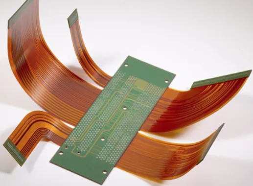
The Cost Effective Guide to Rigid Flex PCB Design: Optimizing Materials and Manufacturing Processes
Discover practical strategies to lower rigid-flex PCB costs through smart material selection (polyimide, FR4, adhesiveless) and streamlined manufacturing. Learn design best practices, DFM tips, and ROI maximization for medical, aerospace, and wearable applications.


