 00:56
00:56
Copper Thickness
Copper thickness is a critical parameter in printed circuit board (PCB) design and manufacturing, referring to the weight of copper per unit area on the board's layers, typically measured in ounces per square foot (oz/ft²). Standard values range from 0.5 oz to 4 oz or more, directly influencing the board's electrical conductivity, thermal management, and mechanical strength. For engineers and electronics enthusiasts searching for information on copper thickness, this tag aggregates articles that delve into its implications for high-current applications, signal integrity, and overall PCB reliability. Understanding copper thickness helps in optimizing designs to prevent issues like overheating or voltage drops in power electronics. For instance, a 1 oz copper layer is common for low-power circuits, while thicker options like 2 oz or 3 oz are essential for high-amperage traces in automotive or industrial systems. Practical applications include calculating trace widths based on IPC standards to ensure safe current handling, selecting appropriate thicknesses for multilayer boards to minimize impedance mismatches, and evaluating trade-offs between cost and performance. Best practices involve consulting datasheets for components, using simulation tools to model thermal behavior, and considering fabrication constraints to avoid delamination or etching challenges. By exploring the resources under this copper thickness tag, users can gain actionable insights into real-world scenarios, such as upgrading from standard to heavy copper for LED drivers or troubleshooting failures in dense SMT assemblies. These articles provide detailed explanations, formulas for derating, and case studies that empower informed decision-making in PCB projects.
Video Guide


Technical Articles
The Ultimate Copper Thickness (Mils) Conversion Chart for PCB Design
2oz Copper PCB Cost Analysis: Is the Performance Worth the Premium?
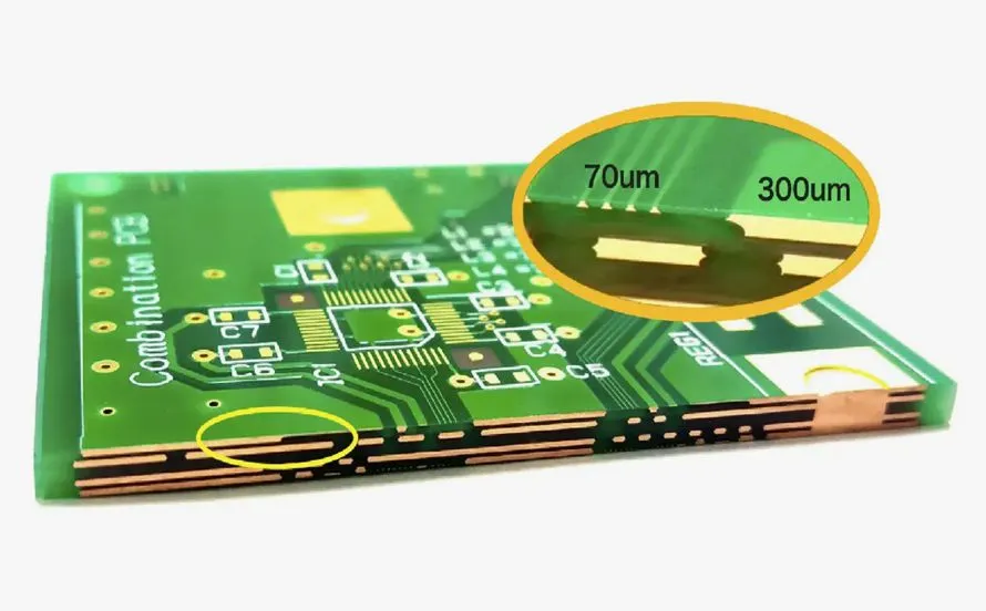
Thermal Performance Showdown: 1oz vs 2oz Copper PCBs for LED Lighting
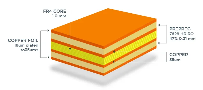
Copper Thickness in Mils: A Comparison of Different PCB Standards (IPC vs. Others)
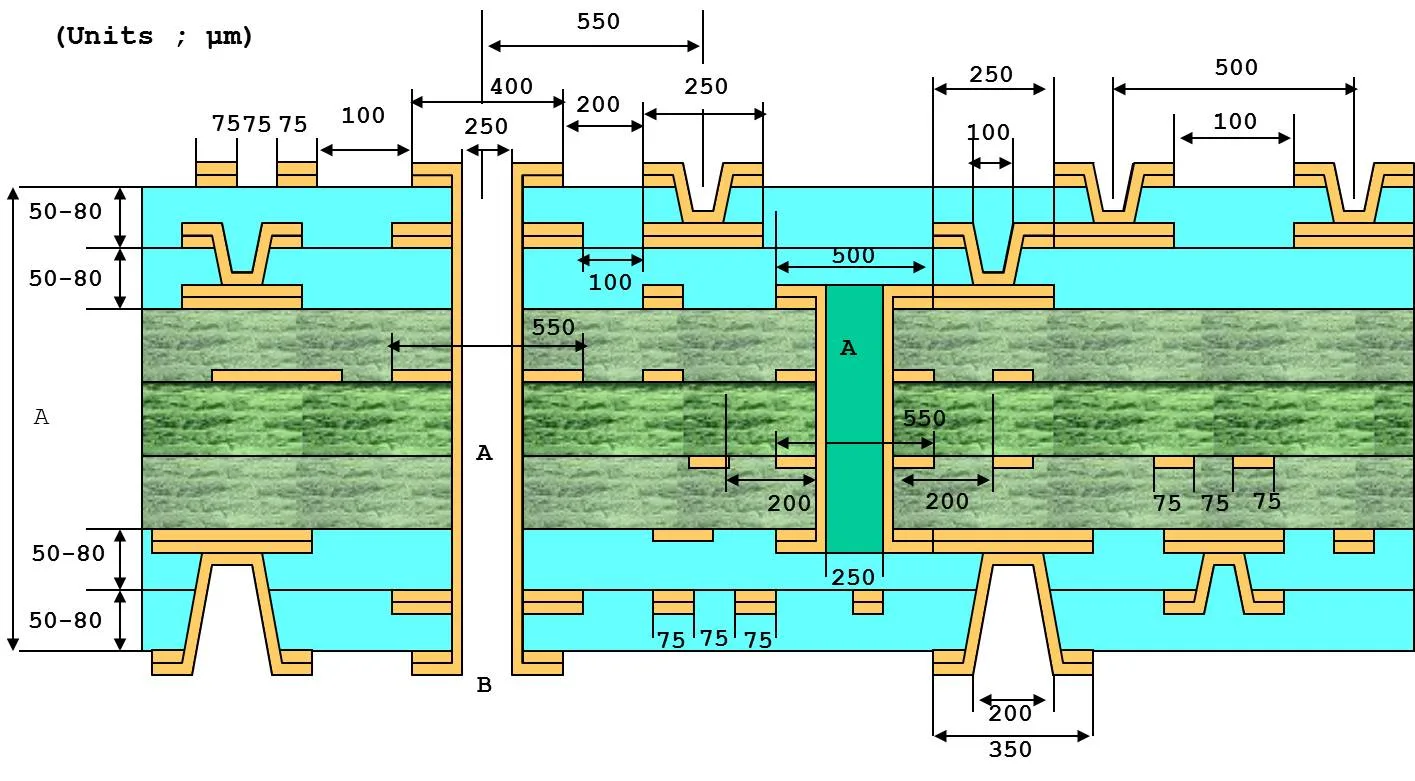
Signal Integrity on a Budget: Choosing the Right Inner Layer Copper Thickness for Hobbyist PCBs
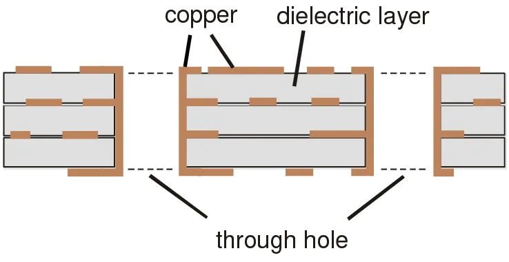
IPC Standards Demystified: Inner Layer Copper Thickness Requirements for Reliable PCBs
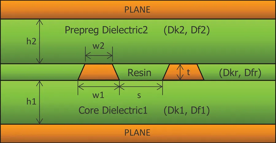
Copper Thickness in Mils and PCB Manufacturing Tolerances: What You Need to Know
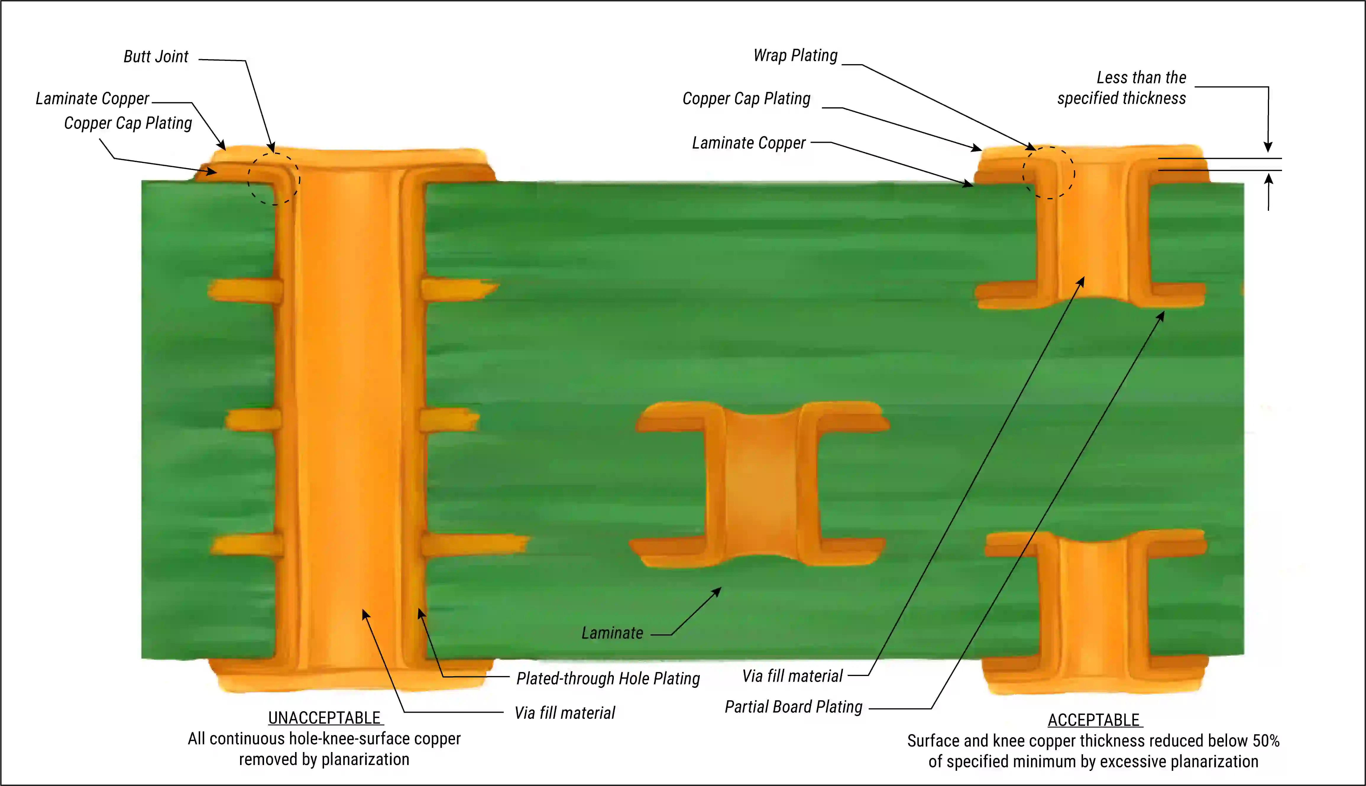
Outer Layer Copper Thickness and Via Design: Best Practices for Reliable PCB Interconnects
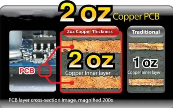
DIY Guide: Modifying Outer Layer Copper Thickness for Improved Thermal Performance in Custom PCBs
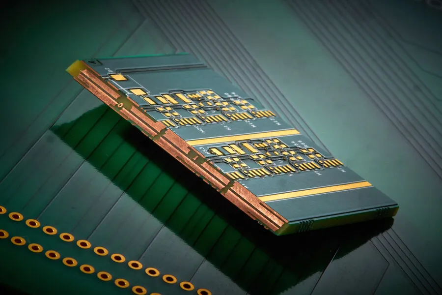
Beyond Standard: Exploring High Outer Layer Copper Thickness PCBs for High Power Applications
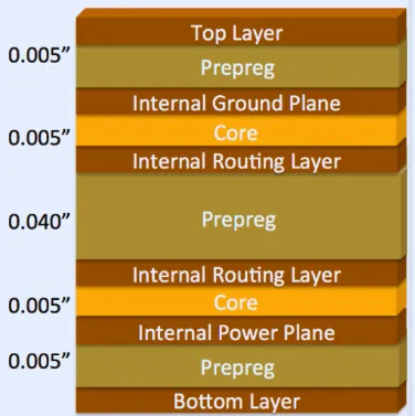
Choosing the Right PCB Layer Thickness: A Comprehensive Guide
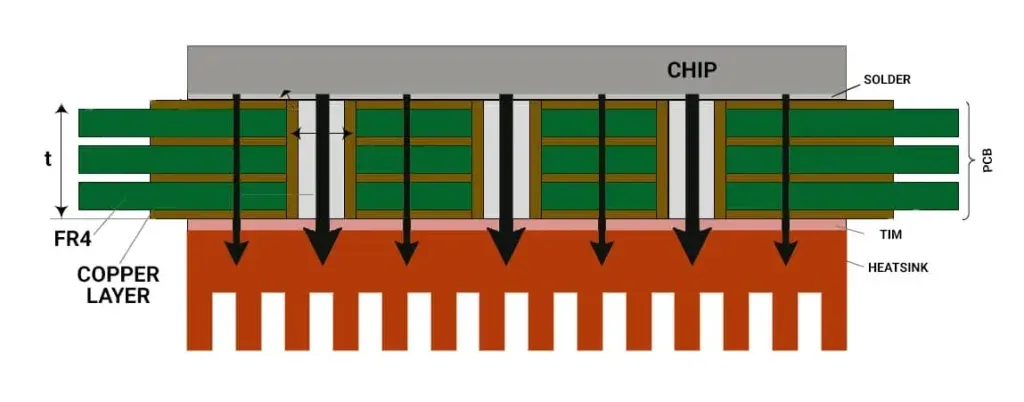
Inner Layer Copper Thickness: A Key to Effective PCB Heat Dissipation
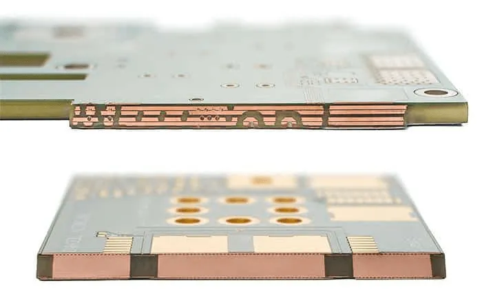
IPC Standards for PCB Copper Weight: Ensuring Quality and Reliability
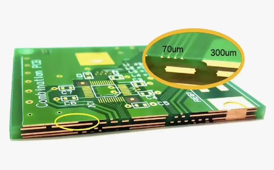
What You Need to Know About Copper Weight in PCB Design
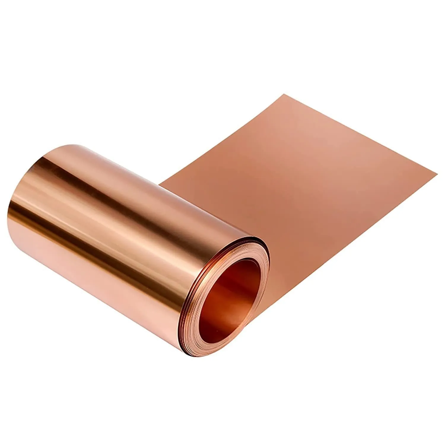
Practical Advantages of High-Tensile, High-Ductility Copper Foil
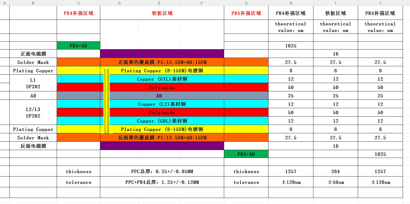
PCB Stackup, Impedance and Thickness Issues in CAM Review
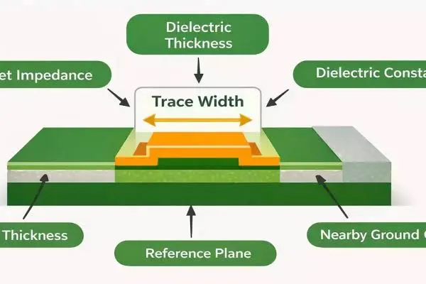
FR4 PCB Minimum Trace Width: What Designers Should Know

FR4 PCB Minimum Trace Spacing: Design Rules and Manufacturing Limits
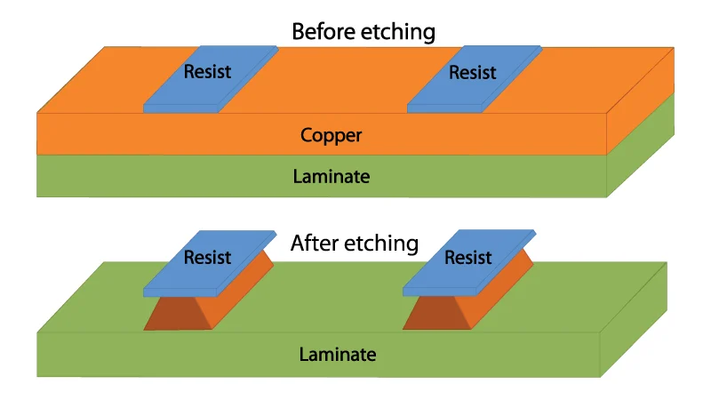
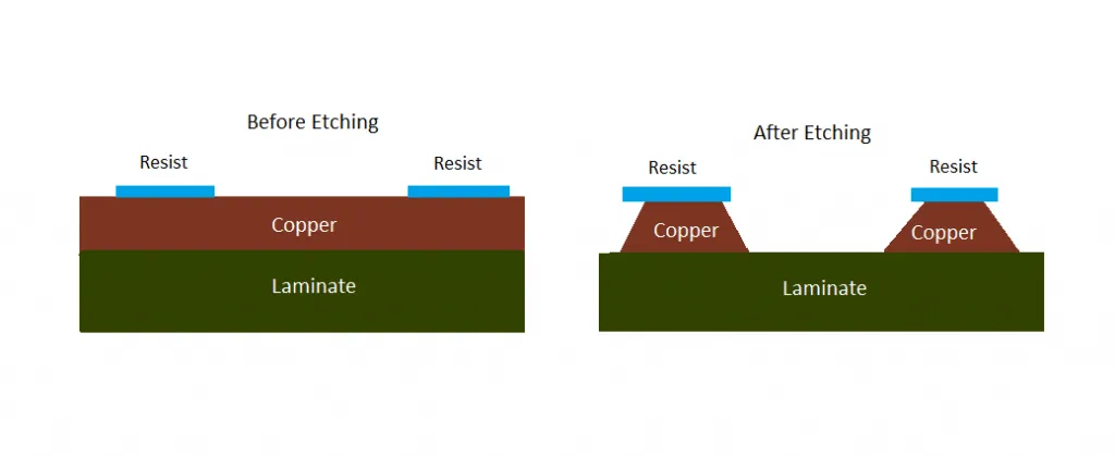
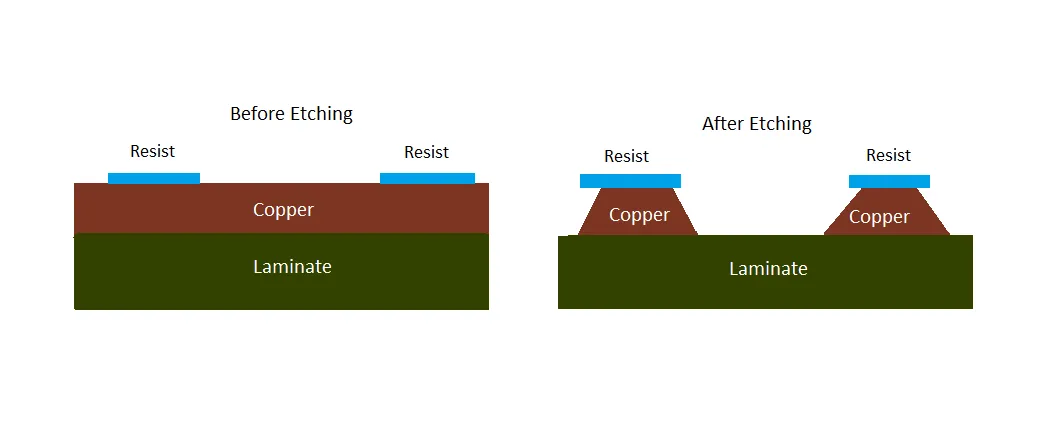
FR4 PCB Etching Undercut: Causes and Process Control